


INSTALLATIONS
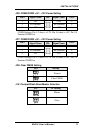
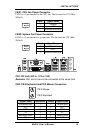
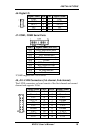
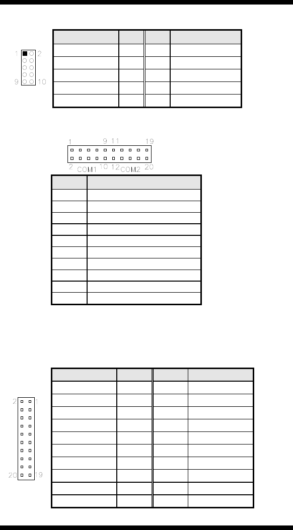
J6: Digital I/O
Signal Name Pin Pin Signal Name
GND 1 2 VCC
OUT3 3 4 OUT1
OUT2 5 6 OUT0
IN3 7 8 IN1
IN2 9 10 IN0
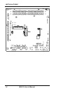
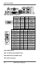
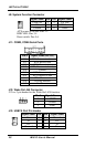
J7: COM1, COM2 Serial Ports
Pin # Signal Name (RS-232)
1/11 DCD, Data carrier detect
3/13 RXD, Receive data
5/15 TXD, Transmit data
7/17 DTR, Data terminal ready
9/19 Ground
2/12 DSR, Data set ready
4/14 RTS, Request to send
6/16 CTS, Clear to send
8/18 RI, Ring indicator
10/20 No Connect.
*COM2 supports RS-232/422/485.
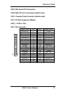
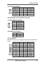
J8, J10: LVDS Connectors (1st channel, 2nd channel)
The LVDS connectors on board consist of the first channel and second
channel and supports 18-bit.
Signal Name Pin # Pin # Signal Name
TX0- 2 1 TX0+
Ground 4 3 Ground
TX1- 6 5 TX1+
5V/3.3V 8 7 Ground
NC 10 9 NC
TX2- 12 11 TX2+
Ground 14 13 Ground
TXC- 16 15 TXC+
5V/3.3V 18 17 ENABKL
+12V 20 19 +12V
MI810 User’s Manual 19