Intel
®
Solid-State Drive 520 Series
Intel
®
Solid-State Drive 520 Series
Product Specification February 2012
14 Order Number: 325968-001US
Intel
®
Solid-State Drive 520 Series
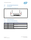
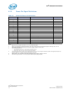
4.2.2 Power Pin Signal Definitions
Notes:
1. All pins are in a single row, with a 1.27 mm (0.050-inch) pitch.
2. Pins P1, P2 and P3 are connected together; Pins P13, P14 and P15 are connected together. Although they are not
connected internally to the device, the host may apply voltage on these pins.
3. The mating sequence is:
• Ground pins P4-P6, P10, P12 and the 5V power pin P7.
• Signal pins and the rest of the 5V power pins P8-P9.
4. Ground connectors P4 and P12 may contact before the other 1st mate pins in both the power and signal connectors to
discharge ESD in a suitably configured backplane connector.
5. Power pins P7, P8, and P9 are internally connected to one another within the device.
6. The host may ground P11 if it is not used for Device Activity Signal (DAS).
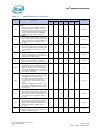
Table 10. Serial ATA Power Pin Definitions
Pin
1
Name Definition Mating Order
P1
2
V
33
3.3 V Power; not used 2nd Mate
P2
2
V
33
3.3 V Power; not used 2nd Mate
P3
2
V
33
3.3 V Power; not used 1st Mate
P4
3,4
Ground 1st Mate
P5
3
Ground 1st Mate
P6
3
Ground 1st Mate
P7
3,5
V
5
5 V Power 1st Mate
P8
3,5
V
5
5 V Power 2nd Mate
P9
3,5
V
5
5 V Power 2nd Mate
P10
3
Ground 1st Mate
P11
6
DAS Device Activity Signal 2nd Mate
P12
3, 4
Ground 1st Mate
P13
2
V
12
12 V Power; not used 1st Mate
P14
2
V
12
12 V Power; not used 2nd Mate
P15
2
V
12
12 V Power; not used 2nd Mate


