Intel® Solid-State Drive DC S3500
December 2013 Product Specification
328860-002US 19
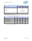
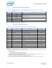
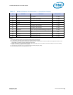
Table 17. Serial ATA Power Pin Definitions—1.8-inch Form Factors
Pin Function Definition Mating Order
1
P1
2
V
33
3.3 V Power
2
nd
Mate
P2
2
V
33
3.3 V Power, per-charge
2
nd
Mate
P3
3
Ground
--
1
st
Mate
P4
3
Ground
--
1
st
Mate
P5
4
V
5
5 V Power; not connected.
1
st
Mate
P6
4
V
5
5 V Power; not connected.
2
nd
Mate
P7
5
DAS/DSS
Device Activity Signal/Disable Staggered Spin-up
2
nd
Mate
Key
Key
NC
NC
P8
6
Optional
Manufacturing Test Pin
2
nd
Mate
P9
6
Optional
Manufacturing Test Pin
2
nd
Mate
Notes:
1. All mate sequences assume zero angular offset between connectors.
2. P1 and P2 are internally connected to one another within the device.
3. Ground connectors P3 and P4 may contact before the other 1st mate pins in both the power and signal connectors to dis-
charge ESD in a suitably configure backplane connector.
4. Pins P5 and P6 are not connected internally to the device but there is an option to connect through a zero ohm stuffing
resistor. The host may put 5V on these pins.
5. The host may ground P7 if it is not used for Device Activity Signal (DAS).
6. P8 and P9 should not be connected by the host.


