


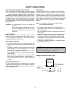
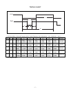
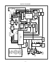
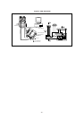

DESCRIPTION OF BLOCK DIAGRAM
- 11 -
1. SMPS(Switching Mode Power Supply)
When you turn on the power switch, the operating
fprocedure is as follows:
.
6. X-RAY Protection Circuit
When the high Voltage reaches to 29kV in an abnormal case,
the high voltage detector circuit, R818,D721,C739-1 R416,
C409 start operation to shut down high voltage circuit.
7. Horizontal S-correction Circuit.
This circuit corrects the horizontal linearity for each horizontal
sync frequency.
8. Horizontal drive and Output Circuit.
This circuit is a horizontal deflection amplifier for raster scan.
9. ABL Circuit
This circuit limits the beam-current for the reliability of CDT
10. Vertical Output Circuit
This circuit takes the vertical ramp wave from the TDA4867J
(IC601) and perform the vertical deflection by supplying the
saw-tooth wave current to the vertical deflection yoke.
11. Blanking and Brightness Control Circuit.
Blanking circuit eliminates the retrace line by supplying
a negative pulse wave to the G1 of the CDT.
Brightness control circuit is used for control of the screen
brightness by changing the DC level G1.
12. Image Rotation (Tilt) Circuit.
This circuit corrects the tilt of the screen by supplying
the image rotation signal to the tilt coil which is
attached near the deflection yoke of the CDT.
13. OSD (On Screen Display) Circuit.
This circuit displays information of the monitor`s status
on the screen.
14. Video Processor Circuit.
Video processor circuit consists of the video drive output
block. The video drive IC(IC302) receives the video
signal from PC. The gain of each channel is controlled
by MICOM through IIC.
The cut-off circuit compensate different voltage of each
channel between the cathode and the G1 of the CDT.
1) The AC line voltage is rectified by the bridge diode
D900.
2) The control IC(IC901) starts switching and generates
switch pulse in the primary turn of the SMPS
transformer(T901)
3) The switching pulses of the primary turns are induced
to the secondary turns of the transformer by the turn
ratio. This pulses are rectified by each diode(D971,
D961(D962),D951,D942,D941)
4) Each rectified DC voltage(80V, 50V, 15V,6.3V and 5V)
2. Over Voltage Protection Circuit
When the input of IC901 Vin (pin 4) is more than 22V, all the
secondary voltages of the SMPS transformer (T901) down
to low value
3. Display Power Management Circuit(DPM)
1) DPM OFF
When no input of horizontal or vertical sync Q951,
Q941 are turned off .Then input power consumption
is below 4 watts.
4. Microprocessor Control & Horizontal and Vertical Sync
Processor Circuit
The operating procedure is as follows ;
1) There is Horizontal & Vertical process function in
Microprocessor.(IC401)
2) Microprocessor (IC401) discriminates the operating mode
from the sync polarity and resolution.
3) After microprocessor reads these adjusted mode data
stored at EEPROM, it controls operating mode data through
IIC
4) Users can control screen condition by the OSD Select,Up,
Down, Left, Right, Exit.
5. D/D Converter Circuit.
To obtain constant high voltage, this circuit supplies
controlled DC voltage for FBT and horizontal deflection
circuit according to the horizontal sync frequency.