


2-6 2 Gbit/s Host Adapter Characteristics
Ver. 2.0 Copyright © 2002 by LSI Logic Corporation. All rights reserved.
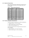
2.3.3 Electromagnetic Compliance
These boards are designed and implemented to minimize
electromagnetic emissions, susceptibility, and the effects of
electromagnetic discharge. The boards are tested to comply with Class B
and carry markings for CE, VCCI, Canada, C-Tick, and FCC.
2.3.4 Safety Characteristics
The bare boards meet the requirements of flammability rating UL 94 V-0.
The bare boards are also marked with the supplier’s name or trademark,
type, and UL flammability rating. Since these boards are installed in a
PCI bus slot, all voltages are below the SELV 42.4 V limit.
2.4 Operational Environment
Use the LSI Logic 2 Gbit/s Fibre Channel to PCI host adapter in PCI
computer systems. The LSI Logic supplied FC BIOS and firmware
operate the boards. An on-board flash memory device and a serial
EEPROM are provided to allow BIOS code and open boot code support
through PCI.
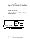
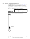
2.4.1 The PCI Interface
The PCI interface operates as a 64-bit DMA bus master. Edge connector
J1 makes the PCI connection, which provides connections on both the
front and back of the board. The signal definitions and pin numbers
conform to the PCI Local Bus Specification, Revision 2.2. See that
specification for more details regarding the signal assignments. The
on-board regulators provide power to the board’s 3.3 V devices.
Note: The PCI +3.3 V pins are tied together and decoupled with
high frequency bypass capacitors to ground. No current
from these +3.3 V pins is used on the board. The board
derives power from the +5 V pins, directly and through a
3.3 V voltage regulator. The PCI +3 V/+5 V pins are used
to differentiate between a 5 V or a 3.3 V PCI signaling
environment.