


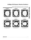
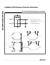
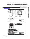
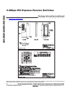
MAX4888A/MAX4889A
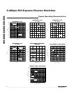
5.0Gbps PCI Express Passive Switches
2 _______________________________________________________________________________________
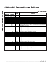
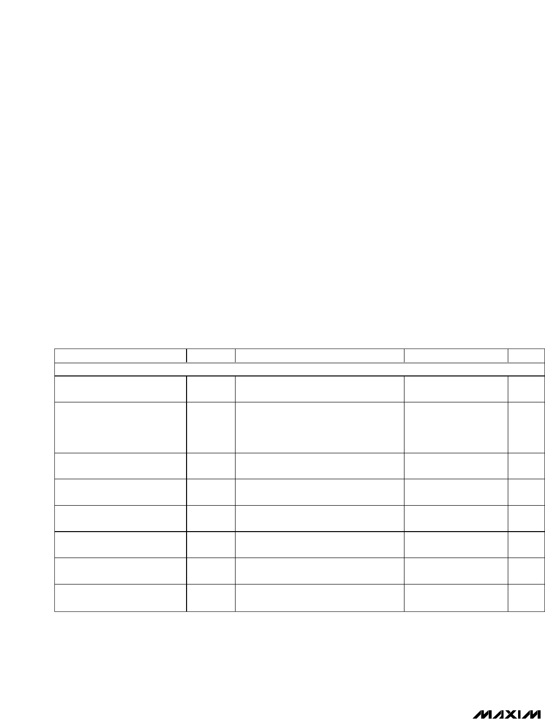
ABSOLUTE MAXIMUM RATINGS
ELECTRICAL CHARACTERISTICS
(V+ = 3.0V to 3.6V, T
A
= -40°C to +85°C, unless otherwise noted. Typical values are at V+ = 3.3V, T
A
= +25°C.) (Note 2)
Stresses beyond those listed under “Absolute Maximum Ratings” may cause permanent damage to the device. These are stress ratings only, and functional
operation of the device at these or any other conditions beyond those indicated in the operational sections of the specifications is not implied. Exposure to
absolute maximum rating conditions for extended periods may affect device reliability.
(All voltages referenced to GND, unless otherwise noted.)
V+.............................................................................-0.3V to +4V
SEL, COM__, NO__, NC__ (Note 1) .............-0.3V to (V+ + 0.3V)
| COM__ - NO__ |, | COM__ - NC__ | (Note 1)...................0 to 2V
Continuous Current (COM_ to NO__/NC__) .....................±70mA
Peak Current (COM__ to NO__/NC__)
(pulsed at 1ms, 10% duty cycle)..................................±70mA
Continuous Current (SEL).................................................±30mA
Peak Current (SEL)
(pulsed at 1ms, 10% duty cycle)................................±150mA
Continuous Power Dissipation (T
A
= +70°C)
28-Pin TQFN (derate 20.8mW/°C above +70°C) ....1666.7mW
42-Pin TQFN (derate 35.7mW/°C above +70°C) ....2857.1mW
Operating Temperature Range ...........................-40°C to +85°C
Storage Temperature Range.............................-65°C to +150°C
Lead Temperature (soldering, 10s) .................................+300°C
Junction Temperature......................................................+150°C
PARAMETER SYMBOL CONDITIONS MIN TYP MAX UNITS
ANALOG SWITCH
Analog-Signal Range
V
COM_
,
V
NO_
,
V
NC_
-0.1 (V+ - 1.2) V
Voltage Between COM and
NO/NC
| V
COM_
-
V
NO_
| ,
| V
COM_
-
V
NC_
|
0 1.8 V
On-Resistance R
ON
V+ = 3.0V, I
COM_
= 15mA,
V
NO_
or V
NC_
= 0V, 1.8V
7 Ω
On-Resistance Match Between
Pairs of Same Channel
ΔR
ON
V+ = 3.0V, I
COM_
= 15mA,
V
NO_
or V
NC_
= 0V (Notes 3, 4)
0.1 1 Ω
On-Resistance Match
Between Channels
ΔR
ON
V+ = 3.0V, I
COM_
= 15mA,
V
NO_
or V
NC_
= 0V (Notes 3, 4)
0.6 2 Ω
On-Resistance Flatness R
FLAT
(
ON
)
V+ = 3.0V, I
COM_
= 15mA
V
NO_
or V
NC_
= 0V, 1.8V (Notes 4, 5)
0.06 2 Ω
NO_ or NC_ Off-Leakage
Current
I
NO_
(
OFF
)
I
NC_
(
OFF
)
V+ = 3.6V, V
COM_
= 0V, 1.8V,
V
NO_
or V
NC_
= 1.8V, 0V
-1 +1 µA
COM_ On-Leakage
Current
I
COM_
(
ON
)
V+ = 3.6V, V
COM_
= 0V, 1.8V,
V
NO_
or V
NC_
= V
COM_
or unconnected
-1 +1 µA
Note 1: Signals on SEL, NO__, NC__ or COM__ exceeding V+ or GND are clamped by internal diodes. Limit forward-diode current
to maximum current rating.