


Appendix B – Product Approvals, Regulatory Design Considerations, and Regulatory Compliance
Multi-Tech Systems, Inc. SocketModem MT5600SMI Developer’s Guide 121
Other Design Considerations
Good engineering practices must be adhered to when designing a printed circuit board (PCB) containing
the SocketModem module. Suppression of noise is essential to the proper operation and performance of
the modem itself and for surrounding equipment.
Two aspects of noise in an OEM board design containing the SocketModem must be considered: on-
board/off-board generated noise that can affect digital signal processing. Both on-board and off-board
generated noise that is coupled on-board can affect interface signal levels and quality. Of particular
concern is noise in frequency ranges affecting modem performance.
On-board generated electromagnetic interference (EMI) noise that can be radiated or conducted off-board
is a separate, but equally important, concern. This type of noise can affect the operation of surrounding
equipment. Most local government agencies have stringent certification requirements that must be met for
use in specific environments.
Proper PC board layout (component placement, signal routing, trace thickness and geometry, etc.)
component selection (composition, value, and tolerance), interface connections, and shielding are
required for the board design to achieve desired modem performance and to attain EMI certification.
The aspects of proper engineering practices are beyond the scope of this designer guide. The designer
should consult noise suppression techniques described in technical publications and journals, electronics
and electrical engineering text books, and component supplier application notes.
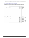
PC Board Layout Guidelines
In a 2-layer design, provide an adequate ground grid in all unused space around and under
components on both sides of the board and connect in such a manner as to avoid small islands. A
grid is preferred over a solid plane to improve solderability. Typically, the grid is composed of 0.012-
inch traces and 0.012- inch spaces on a 0.025-inch grid. Connect each grid to other grids on the
same side at several points and grids on the opposite side through the board at several points.
In a 4-layer design, provide adequate ground plane covering the entire board. In 4-layer designs,
power and ground are typically on the inner layers. All power and ground traces should be 0.05
inches wide.
Tip and Ring signal traces are to be no closer than 0.062 inches to any other traces for U.S.
applications. Tip and Ring signal traces are to be no closer than 0.078 inches (2.0 mm) from any
other traces or ground circuits for European applications. 2.0 mm spacing must be used if the host
board is to support both U.S. and European SocketModem applications.
If the SocketModem is mounted flush with the host PCB, the host PCB should be clear of all traces
directly underneath the SocketModem oscillator section (under the chip). It is strongly recommended
that the SocketModem be mounted at least 0.130 inch above the host PCB.
The recommended hole size for the SocketModem pins is 0.036 in. +/-0.003 in. in diameter. Spacers
can be used to hold the SocketModem vertically in place during the wave solder process. A spacer
should be placed on pin 32 and pin 64 of the SocketModem. A suggested part number for the spacer
is BIVAR 938-0.130 for P1(0.310in) option SocketModems. The spacers can be left on permanently
and will not effect operation.