Chapter 4 – SocketModem Parallel Interface – A Programmer's Description
Multi-Tech Systems, Inc. SocketModem MT5600SMI Developer’s Guide 26
MSR – Modem Status Register (Addr = 6)
The Modem Status Register (MSR) reports current state and change information of the modem. Bits
4-7 supply current state, and bits 0-3 supply change information. The change bits are set to a 1
whenever a control input form the modem changes state from the last MSR read by the host. Bits 0-3
are reset to 0 when the host reads the MSR or upon reset.
Whenever bits 0, 1, 2, or 3 are set to a 1, a Modem Status Interrupt (IIR0-IIR3 = 0) is generated.
Bit 7 Data Carrier Detect (DCD)
This bit indicates the logic state of the DCH# (RLSD#) output. If Loopback is selected (MCR4 =
1), this bit reflects the state of the Out2 bit in the MCR (MCR3).
Bit 6 Ring Indicator (RI)
This bit indicates the logic state of the RI# output. If Loopback is selected (MCR4 = 1), this bit
reflects the state of the Out1 bit in the MCR (MCR2).
Bit 5 Data Set Ready (DSR)
This bit indicates the logic state of the DSR# output. If Loopback is selected (MCR4 = 1), this bit
reflects the state of the DTR in the MCR (MCR0).
Bit 4 Clear to Send (CTS)
This bit indicates the logic state of the CTS# output. If Loopback is selected (MCR4 = 1), this bit
reflects the state of the RTS bit in the MCR (MCR1).
Bit 3 Delta Data Carrier Detect (DDCD)
This bit is set to a 1 when the DCD bit changes state since the host last read the MSR.
Bit 2 Trailing Edge of Ring Indicator (TERI)
This bit is set to a 1 when the RI bit changes from a 1 to a 0 state since the host last read the
MSR.
Bit 1 Delta Data Set Ready (DDSR)
This bit is set to a 1 when the DSR bit has changed since the host last read the MSR.
Bit 0 Delta Clear to Send (DCTS)
This bit is set to a 1 when the CTS bit has changed since the MSR the host last read the MSR.
RBX – RX Buffer (Receiver Buffer Register) (Addr = 0,
DLAB = 0)
The RX Buffer (RBR) is a read-only register at location 0 (with DLAB = 0). Bit 0 is the least significant
bit of the data and is the first bit received.
THR – TX Buffer (Transmitter Holding Register) (Addr = 0,
DLAB = 0)
The TX Buffer (THR) is a write-only register at address 0 when DLAB = 0. Bit 0 is the least significant
bit and the first bit sent.
Divisor Registers (Addr = 0 and 1, DLAB = 1)
The Divisor Latch LS (least significant byte) and Divisor Latch MS (most significant byte) are two
read-write registers at locations 0 and 1 when DLAB = 1, respectively.
The baud rate is selected by loading each divisor latch with the appropriate hex value.
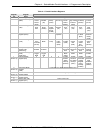
Programmable values corresponding to the desired baud rate are listed in Table 4-3.


