


TLF5012
The DP8400 Family of Memory Interface Circuits AN-302
National Semiconductor
Application Note 302
Charles Carinalli
Mike Evans
February 1986
The DP8400 Family of
Memory Interface Circuits
INTRODUCTION
The rapid development in dynamic random access memory
(DRAM) chip storage capability coupled with significant
component cost reductions has allowed designers to build
large memory arrays with high performance specifications
However the development of memory arrays continues to
have a common set of problems generated by the complex
timing and refresh requirements of DRAMs These include
how to quicklydrive thememories to takeadvantage of their
speed minimization of board space required by the support
circuitry and the need for error detection and correction
Unfortunately theseproblems must beaddressed with each
new system design Full system solutions will vary greatly
depending on the DRAM arraysize memory speed and the
processor
This application note introducesa complete family of DRAM
support circuits that provides a straightforward solution to
the above problems while allowing a high degree of flexibili-
ty in application with little or no performance penalty The
DP8400 family (Table I) includes DRAM controllers error
detectioncorrection circuits octal address buffers and sys-
tem control circuits The LSI blocks are designed with flex-
ible interfaces making application possible with all existing
DRAMs including the recently announced 1 Mbit devices
Additionally interface is easyto all popular microprocessors
with memory word widths possible from 8 to 80 bits
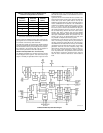
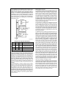
TABLE IDP8400 Family Members
DP8400-2 16 and32 Bit Error
DP8402A CheckerCorrectors
DP8408A DP8409A DRAM ControllerDrivers
DP8417 DP8418
DP8419 DP8428DP8429
DP8420 DP84244 DRAM BufferDrivers
DP84XX2 Microprocessor
Interface Circuits
FULL FUNCTIONDRAM CONTROLLER
The heart of any DRAM array design is the controller func-
tion Previous LSI controllers supplied a minimum function
of address multiplexing with an on-board refresh counter
This required external delay line timing and logic to control
memory access additionallogic to perform memoryrefresh
and external drivers to drive the capacitive memory array
The complete solution results in significant access delay in
relation to DRAM speeds and skews in output sequencing
as well as a large component count
A previous LSI solution brought much of this logic on-chip
However it is limited in application to certain microproces-
sors and has the disadvantage of all access timing originat-
ing from an external clock whose phase uncertainty gener-
ates a delay in actually knowing when an access has start-
ed
The DP8409A multi-mode dynamic RAM controllerdriver
was the first controller to resolve all ofthese problems This
Schottky bipolar device provides the flexibility of external
access control along with automatic access timing genera-
tion without theneed for an externaltiming generator clock
In addition on-board capacitive drivers allow direct drive for
over 88 DRAMs With the simple addition of refresh clocks
the circuit can perform hiddenrefresh automatically It is the
DP8409A design that has beenused as the spring board for
a whole family of controllers with faster speed performance
while maintaining maximum pin upgrade compatibility
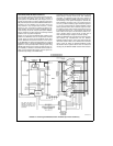
All Control On-Chip
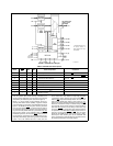
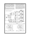
Figure 1
is a block diagram of the DP8409A the ADS input
strobes the parallel memory address into the row latches
R0–8 the column latches C0–8 and bank select B0 and
B1 The nine outputdrivers may be multiplexedbetween the
row or column input latches or the 9-bit on-chip refresh
counter One of four RAS
outputs is selected during an ac-
cess cycle by setting the bank select inputs B0 or B1 All
four RAS
outputs are active during refresh Either external
or automatic control is available on-chip for the CAS
output
while an on-chip buffer is provided to minimizeskew associ-
ated with WE
output generation
All DRAM address and controloutputs on the DP8409A can
directly drive in excess of 500 pF or the equivalent of 88
DRAMs (4 banks of 22 DRAMs) All output drivers are
closely matched significantly reducing output skew Each
output stage has symmetrical high and low logic level drive
capability insuring matched rise and fall time characteris-
tics
Flexibility and Upgradability to 256k or 1 Mbit DRAMs
The 9 multiplexed address outputs and 9-bit internal refresh
counter of the DP8409A direct addressing capability for
256k DRAMs Careful design of memory boards using 64k
DRAMs with the DP8409A insures direct upgradability to
256k DRAMs Thiscan be doneby simply allowingfor board
address extension by two bits and designing the ninth ad-
dress trace (Q8) of the DP8409A to connect to pin 1 of the
DRAMs (A8) This is in general a non-connected pin in
64ks and the ninth address in 256ks All that need be done
is to remove the 64ks and replace themwith 256ks thereby
increasing the memory on the same board bya4to1ratio
The resulting development cost saving can be significant
Although the new 1 Mbit DRAMs require the larger 18 pin
package which will require a memory board redesign up-
grading the controller portion of the board may need no
redesign when converting from the DP8409A or DP8419 to
the new DP8429 1 Mbit DRAM controller driver
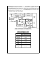
Three mode pins (M0 M1 and M2) offer externally select-
able modes of operation a key reason for the DP8409A’s
application flexibility (Table II) The operational modes are
divided between external and automatic memory control
C
1995NationalSemiconductorCorporation RRD-B30M115PrintedinUSA