


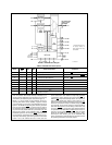
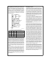

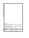
TABLE IVCheck Bit Overheadfor Multiple BitError
Detection andSingle Bit ErrorCorrection
Number ofBits Number of Percentage
in Memory Check Bits of Excess
Data Word Required Memory
8 5 63%
16 6 38%
24 6 (7) 25% (29%)
32 7 22%
48 7 (8) 15% (17%)
64 8 13%
Note The number stated assumes the use of the DP8400 the number in
parentheses is requiredby other error correctioncircuits
lists the number of additional memorychips required to sup-
port single bit error correction and double bit error detection
as a function of the memory data word width
This table also shows the percentage of DRAM overhead
required to implement this function Adding error correction
also increases the memory accessdelay since the informa-
tion contained in the overhead chips must be analyzed in
each read and generated in each write operation
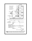
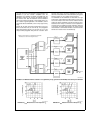
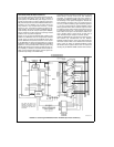
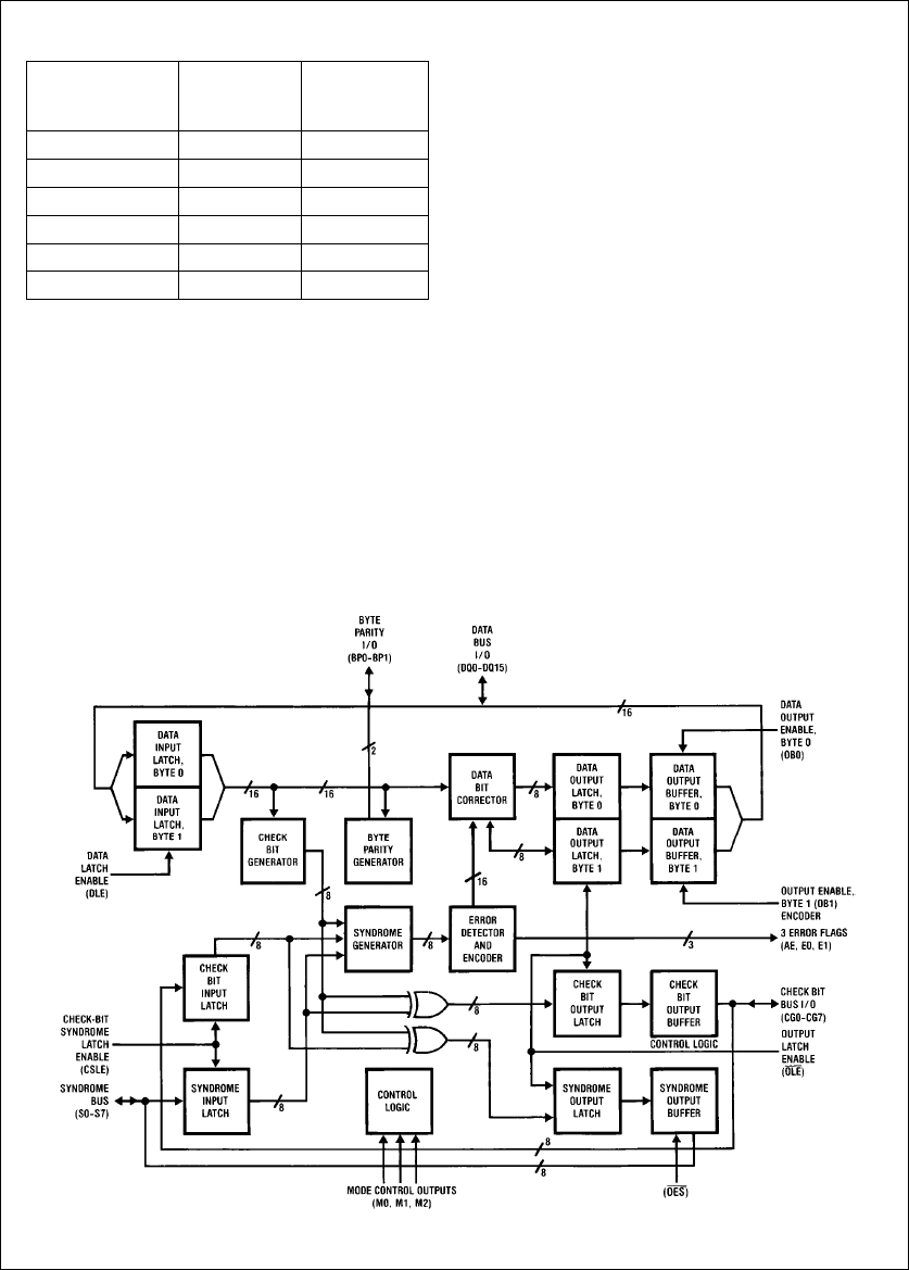
DP8400 16-Bit Expandable Error Correction Chip
The DP8400 expandable error checkercorrector is shown
in block diagram form in
Figure 8
This circuit offers a high
degree of flexibility in applications which range from 8-bit
to 80-bit data words It is a 16-bit chip that is easily expand-
able with the simple addition of more DP8400s for each 16-
bit word increment
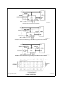
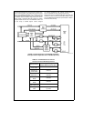
Figures 9a 9b
and
9c
demonstrate its basic operationin the
write and read memory access cycles
Figure 9a
shows the
normal write cycle where system data is used by the
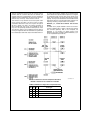
DP8400 to generate parity bits called check bits based on
certain combinations of the data bits This combination is
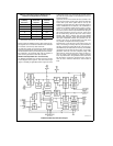
defined by the DP8400’s matrix shown in
Figure 10
When-
ever a ‘‘1’’ occurs in any row the corresponding input data
bit at the top of the column helps determine the parity for
that check bit labeled at the end of the row These check
bits are written along with the data at the same memory
address Also during a memory write cycle the DP8400
checks system byte parity This is parity associated with the
data bytes transmitted between the processor and the
memory card This is an optional feature that may prove
very valuable in multiple board memory systems
Sometime later a read will occur at this same memory ad-
dress The reading of memory data may be performed in
two ways as shown in
Figures 9b
and
9c
In the read cycle
the DP8400 uses the data read from memory and internally
regenerates check bits using the same matrix These newly
generated check bits are then compared (using X-OR
gates) with the check bits read from memory to detect er-
rors The result of this comparison is called a syndrome
word Any differences in the generated versus read check
bits will result in at least one syndrome bit true This indi-
cates an error in either the read data or check bit field or
both
TLF5012–10
FIGURE 8DP8400 Simplified BlockDiagram
7