


Chapter 1 Introduction
© National Instruments Corporation 1-3 NI 781xR User Manual
Overview of Reconfigurable I/O
This section explains reconfigurable I/O and describes how to use the
LabVIEW FPGA Module to build high-level functions in hardware.
Refer to Chapter 2, Hardware Overview of the NI 781xR, for descriptions
of the I/O resources on the NI 781xR.
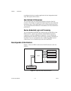
Reconfigurable I/O Concept
The NI 781xR is based on a reconfigurable FPGA core surrounded by fixed
digital input and output resources. You can configure the behavior of the
FPGA to meet the requirements of your measurement and control system.
You can implement this user-defined behavior as an FPGA VI to create an
application-specific I/O device.
Flexible Functionality
Flexible functionality allows the NI 781xR to match individual application
requirements and to mimic the functionality of fixed I/O devices. For
example, you can configure an R Series device in one application for three
32-bit quadrature encoders and then reconfigure the R Series device in
another application for eight 16-bit event counters.
You also can use the R Series device with the LabVIEW Real-Time
Module in timing and triggering applications, such as control and
hardware-in-the-loop (HIL) simulations. For example, you can configure
the R Series device for a single timed loop in one application and then
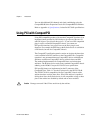
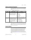
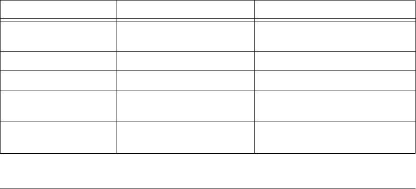
Table 1-1. Pins Used by the NI PXI-781xR
NI PXI-781xR Signal PXI Pin Name PXI J2 Pin Number
PXI Trigger<0..7> PXI Trigger<0..7> A16, A17, A18, B16, B18, C18,
E16, E18
PXI Clock 10 MHz PXI Clock 10 MHz E17
PXI Star Trigger PXI Star Trigger D17
LBLSTAR<0..12> LBL<0..12> A1, A19, C1, C19, C20, D1, D2,
D15, D19, E1, E2, E19, E20
LBR<0..12> LBR<0..12> A2, A3, A20, A21, B2, B20, C3,
C21, D3, D21, E3, E15, E21