Chapter 1 Introduction
© National Instruments Corporation 1-5 R Series Intelligent DAQ User Manual
Reconfigurable I/O Architecture
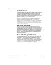
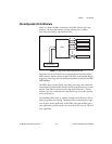
Figure 1-1 shows an FPGA connected to fixed I/O resources and a bus
interface. The fixed I/O resources include A/D converters (ADCs),
D/A converters (DACs), and digital I/O lines.
Figure 1-1. High-Level FPGA Functional Overview
Software accesses the R Series device through the bus interface, and the
FPGA connects the bus interface and the fixed I/O to make possible timing,
triggering, processing, and custom I/O measurements using the LabVIEW
FPGA Module.
The FPGA logic provides timing, triggering, processing, and custom I/O
measurements. Each fixed I/O resource used by the application uses a small
portion of the FPGA logic that controls the fixed I/O resource. The bus
interface also uses a small portion of the FPGA logic to provide software
access to the device.
The remaining FPGA logic is available for higher-level functions such as
timing, triggering, and counting. The functions use varied amounts of logic.
You can place useful applications in the FPGA. How much FPGA space
your application requires depends on your need for I/O recovery, I/O, and
logic algorithms.
FPGA
Bus Interface
Fixed I/O Resource
Fixed I/O Resource
Fixed I/O Resource
Fixed I/O Resource


