


Revision 0.2 (Confidential) 11 www.national.com
LMX9820ADEV: LMX9820A Simply Blue Module Kit User’s Guide
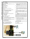
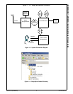
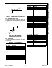
2.2.5 J3 SMA RF Signal Connector
Connect antenna or test equipment to the SMA.
Figure 2-3. J3 SMA Connection - Single TX/RX
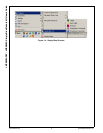
2.2.6 J5 Optional External Clock
An optional external clock can be used. C29, 100 pF, must
be placed for proper operation. It is recommended to set
the signal generator to 12 MHz @ 2 dBm output. Refer to
Figure 2-4.
Figure 2-4. J5 SMA Connection -
(Optional) External Clock Input
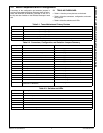
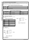
2.2.7 J1 Connector
J1 is a 50-pin board-to-board connector. See Table 2-23 for
pin assignments.
Table 2-23. J1 Pin Assignments
Pin #
Signal
Name Description
1 TMS JTAG - Test Mode Select input
2 D+ USB DATA+
3 TDI JTAG - Test Data input
4 D- USB DATA-
5 TDO JTAG - Test Data output
6
UVCC UVCC
7 TCK JTAG - Test Clock input
8 GND Ground
9 RDY# JTAG - Ready output (active low)
10
VCC VCC
11 GND Ground
12 GND Ground
13 SCK AAI - Clock
14 IOVCC
IOVCC
15 SFS AAI - Frame Synchronization
16 GND Ground
C1
10 pF
J3
SMA
RF_SIGNAL
J5
100 pF
Ext Clk
C29
17 STD AAI - Transmit Data output
18 NC No Connect
19 SRD AAI - Receive Data input
20 NC No Connect
21 GND Ground
22 GND Ground
23 RESET# Reset for LMX5100
24 NC No Connect
25 LSTAT_0 Link Status Bit 0 output
26 GND Ground
27 LSTAT_1 Link Status Bit 1 output
28 NC No Connect
29 ENV0 Module Operating Environment Input Bit 0
30 GND Ground
31 ENV1 Module Operating Environment Input Bit 1
32 TIO3_BB Internal use only
33 SDAT Serial Data
34 GND Ground
35 GND Ground
36 RDX UART Receive Data input
37 ISEL2 Interface Select 2
38 TDX UART Transport - Transmit Data
39 ISEL1 Interface Select 1
40 CTS# UART Transport - Clear-to-Send
41 TIO4_BB Internal use only
42 RTS# UART Transport - Request-to-Send
43 GPIO1_RF Internal use only
44 GND Ground
45 GPIO2_RF Internal use only
46 RFDATA RF Antenna Port - 50Ω nominal
impedance
47 GND Ground
48 GND Ground
49 GND Ground
50 TR Switch TR Switch
Table 2-23. J1 Pin Assignments (Continued)
Pin #
Signal
Name Description