


359
CHAPTER 17 SERIAL INTERFACE CHANNEL 0 (
µ
PD78058FY SUBSERIES)
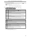
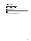
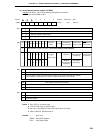
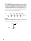
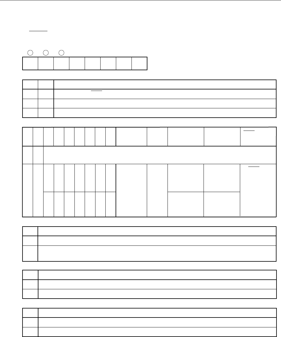
(a) Serial operating mode register 0 (CSIM0)
CSIM0 is set with a 1-bit or 8-bit memory manipulation instruction.
RESET input sets CSIM0 to 00H.
Notes 1. Bit 6 (COI) is a read-only bit.
2. Can be used freely as port function.
3. Be sure to set WUP to 0 when the 2-wire serial I/O mode.
4. When CSIE0=0, COI becomes 0.
Remark × : don’t care
PMXX : Port Mode Register
PXX : Port Output Latch
65432107
Symbol
CSIM0 CSIE0 COI WUP
CSIM04 CSIM03 CSIM02 CSIM01 CSIM00
CSIM01
0
1
Serial Interface Channel 0 Clock Selection
Input Clock to SCK0 pin from off-chip
8-bit timer register 2 (TM2) output
R/W
1 Clock specified with bits 0 to 3 of timer clock select register 3 (TCL3)
CSIM
04
0
CSIM00
×
0
1
FF60H 00H R/W
Note 1
Address After Reset R/W
R/W
CSIM
03
CSIM
02
PM25 P25 PM26 P26
PM27
P27
Operation
Mode
Start Bit
SIO/SB0/SDA0
/P25 Pin Function
SO0/SB1/SDA1
/P26 Pin Function
SCK0/SCL/P27
Pin Function
×
WUP
0
1
Wake-up Function Control
Note 3
Interrupt request signal generation with each serial transfer in any mode
Interrupt request signal generation when the address received after detecting start condition
(when CMDD=1) matches the slave address register (SVA) data in I
2
C bus mode
R/W
2-wire serial
l/O mode
or
I
2
C bus mode
0
SCK0/SCL
(N-ch open-drain
input/output)
1
11
×
0
×
0
0
×
0
×
0
0
1
1
Note 2 Note 2
Note 2 Note 2
MSB
P25 (CMOS
input/output
SB0/SDA0
(N-ch open-drain
input/output)
SB1/SDA1
(N-ch open-drain
input/output)
P26 (CMOS
input/output)
3-wired serial I/O mode (see section 17.4.2 3-wire serial I/O mode operation.)
COI
0
Slave Address Comparison Result Flag
Note 4
Slave address register (SVA) not equal to serial I/O shift register 0 (SIO0) data
Slave address register (SVA) equal to serial I/O shift register 0 (SIO0) data
R
1
CSIE0
0
Serial Interface Channel 0 Operation Control
Operation stopped
Operation enabled
R/W
1