


BIOS
Page 4-6
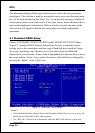
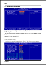
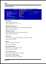
Memory Timings
For setting DRAM Timing.
Options: Optimal, Aggressive, Turbo, Expert.
T (RAS)
This item specifies the number of clock cycles needed after a bank active command
before a precharge can occur (sets the minimum RAS pulse width.).
Options: 1 ~ 15.
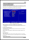
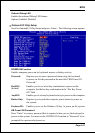
T (RCD)
This item sets the timing parameters for the system memory such as the CAS (Column
Address Strobe) and RAS (Row Address Strobe).
Options: 1 ~ 7.
T (RP)
This item refers to the number of cycles required to return data to its original
location to close the bank or the number of cycles required to page memory before
the next bank activate command can be issued.
Options: 1 ~ 7.
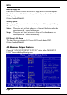
CAS Latency
This item specifies the number of clock cycles needed after a Column Address Strobe
(CAS) signal before data can be read. The default is by DRAM SPD.
Options: 2.0, 2.5, 3.0.
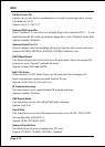
Memory Auto Precharge
Enables Memory Auto Precharge function.
Options: Enabled, Disabled.
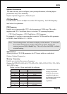
FSB Spread Spectrum
This item can significantly reduce the EMI (ElectroMagnetic Interference) generated
by the CPU.
Options: Disabled, 0.50%, 1.00%.
AGP Spread Spectrum
This item can significantly reduce the EMI (ElectroMagnetic Interference) generated
by the AGP.
Options: Disabled, 0.50%, 1.00%.