C – 10
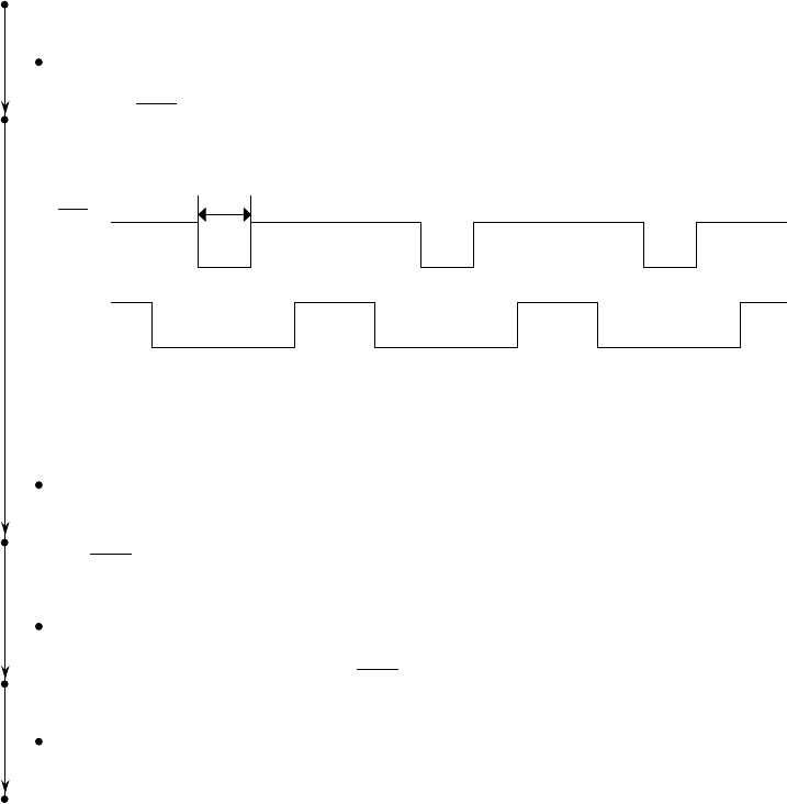
Figure C-3-5
542ns
5V
0V
5V
0V
WR
Q3-3
2 In receiving by serial interface, printing data is omitted or printing operation is not performed.
Are RxD and SSD of Q3 as specified in Figure C-3-4?
No Replace the Q2.
Yes Are, WR, and BUS signals of Q3 pin 3 as specified in Figure C-3-5?
No Replace the Q3.
Yes Is the level of a BUS signals at Q7 pins 2-9 the same as that of DB0-7 when
WR signal is started?
No Replace the Q7.
Yes Is 4 pin of Q6 identical to WR signal in Figure C-3-5?
No Replace the Q6.
Yes Check Q7 (LSI: 10S0210-42) in the SRXD control PCB.


