


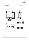

UP05C8PG
2 SJJ00401AED
This product complies with the RoHS Directive (EU 2002/95/EC).
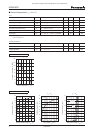
Electrical Characteristics T
a
= 25°C±3°C
Tr
Parameter Symbol Conditions Min Typ Max Unit
Collector-base voltage (Emitter open) V
CBO
I
C
= 100 mA, I
E
= 0 30 V
Emitter-base voltage (Collector open) V
EBO
I
E
= 10 mA, I
C
= 0 3 V
Base-emitter voltage V
BE
V
CE
= 10 V, I
C
= 2 mA 720 mV
Forward current transfer ratio h
FE
V
CE
= 10 V, I
C
= 2 mA 100 250
Transition frequency
*
f
T
V
CB
= 10 V, I
E
= -15 mA, f = 200 MHz 1
300 MHz
Power gain G
P
V
CB
= 10 V, I
E
= -1 mA, f = 100 MHz 20 dB
Note) Measuring methods are based on JAPANESE INDUSTRIAL STANDARD JIS C 7030 measuring methods for transistors.
*
: Pulse measurement
CCD Load Device
Parameter Symbol Conditions Min Typ Max Unit
Pinchi off current I
P
V
DS
= 8 V, V
G
= 0 5.0 7.0 mA
Output impedance Z
O
V
DS
= V, V
G
= 0 0.02 MW
Note) Measuring methods are based on JAPANESE INDUSTRIAL STANDARD JIS C 7030 measuring methods for transistors.
P
T
T
a
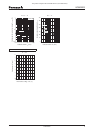
Common characteristics chart
I
C
V
CE
I
C
I
B
I
C
V
BE
Characteristics charts of Tr
0 42 8 106 12
0
18
16
14
20
2
4
12
10
6
8
Collector current I
C
(
mA
)
Collector-emitter voltage V
CE
(
V
)
UP05C8PG_I
C
-V
CE
T
a
= 25°C
I
B
= 100 µA
60 µA
20µA
40µA
80 µA
0 0.4 0.60.2 0.8 1.0
0
40
30
35
45
5
20
25
15
10
Collector current I
C
(
mA
)
Base current I
B
(
mA
)
UP05C8PG_I
C
-I
B
V
CE
= 6 V
0 0.4 0.60.2 1.20.8 1.0 1.4
0
40
50
10
20
30
Collector current I
C
(
mA
)
Base-emitter voltage V
BE
(
V
)
UP05C8PG_I
C
-V
BE
V
CE
= 6 V
T
a
= 85°C
−25°C
25°C
0 40 80 120
0
140
120
100
80
40
20
60
Total power dissipation P
T
(
mW
)
Ambient temperature T
a
(
°C
)
UN05C8PG_P
T
-T
a