


Philips Semiconductors Product specification
TOPFET dual high side switch PIP3202-DC
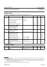
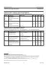
UNDERVOLTAGE & OVERVOLTAGE CHARACTERISTICS
Limits are at -40˚C ≤ T
mb
≤ 150˚C and typicals at T
mb
= 25˚C. Refer to TRUTH TABLE.
SYMBOL PARAMETER CONDITIONS MIN. TYP. MAX. UNIT
Undervoltage
V
BG(UV)
Low supply threshold voltage
1
2 4.2 5.3 V
∆V
BG(UV)
Hysteresis 0.1 0.5 1 V
Overvoltage
V
BG(OV)
High supply threshold voltage
2
35 40 45 V
∆V
BG(OV)
Hysteresis 0.4 1 2 V
I
BG(OV)
Operating current per channel V
BG
> V
BG(OV)
-12mA
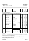
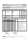
OVERLOAD PROTECTION CHARACTERISTICS
Independent protection per channel. Refer to TRUTH TABLE.
5.5 V ≤ V
BG
≤ 35 V, limits are at -40˚C ≤ T
mb
≤ 150˚C and typicals at T
mb
= 25˚C unless otherwise stated.
SYMBOL PARAMETER CONDITIONS MIN. TYP. MAX. UNIT
Overload protection V
BL
= V
BG
; t
p
= 300 µs
I
L(lim)
Load current limiting V
BG
≥ 8 V 18 30 42 A
V
BG
= 5.5 V 15 27 42 A
Short circuit load protection T
mb
≤ 125˚C prior to overload
3
P
D(TO)
Overload power threshold for latched protection
4
100 150 200 W
T
DSC
Characteristic time which determines trip time
5
- 200 500 µs
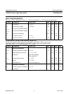
Overtemperature protection
T
j(TO)
Threshold junction temperature 150 170 190 ˚C
∆T
j(TO)
Hysteresis
6
3 1020˚C
1 Undervoltage sensors causes each channel to switch off and reset.
2 Overvoltage sensors causes each output channel to switch off to protect its load.
3 Above this temperature measurement of these parameters is prevented because OT protection may occur prior to SC protection.
4 SC protection for P
D
> P
D(TO)
is latched. Normal operation may only be resumed after the input is toggled low then high again.
Normal operation is maintained as long as P
D
< P
D(TO)
and T
j
< T
j(TO)
.
5 Trip time t
d sc
varies with overload dissipation P
D
according to the exponential model formula t
d sc
≈ T
DSC
/ LN[ P
D
/ P
D(TO)
].
6 After cooling below the reset temperature the channel will resume normal operation.
September 2001 5 Rev 1.000