


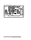

3.1 Accessing the registers
The mode of communication desired is established and monitored through the bit
values of the internal read and write registers. The register set of the SCC includes
16 write registers and 9 read registers. These registers only occupy four address
locations, which start at the MPA-200's physical base address that is configured
via the on board switches. This and all other addresses are referenced from this
base address in the form Base + Offset. An example of this is Base + 1 for the
SCC Control Port, Channel A.
There are two register locations per SCC channel, a data port and a control port .
Accessing the internal SCC registers is a two step process that requires loading a
register pointer to perform the addressing to the correct data register. The first
step is to write to the control port the operation and address for the appropriate
channel. The second step is to either read data from or write data to the control
port. The only exception to this rule is when accessing the transmit and receive
data buffers. These registers can be accessed with the two step process described
or with a single read or write to the data port. The following examples illustrate
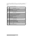
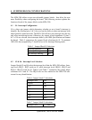
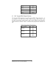
how to access the internal registers of the SCC. Also, Table 2 SCC read register
description describes the read registers and Table 3 SCC write register descrip-
tion describes the write registers for each channel.
The MPA-200 has been designed to assure that all back to back access timing
requirements of the SCC are met without the need for any software timing
control. The standard of adding jmp $+2 between IO port accesses is not required
when accessing the MPA-200.
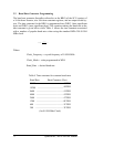
Example 1: Enabling the transmitter on channel A.
mov dx,base ; load base address
add dx,ContA ; add control reg A offset
mov al,05h ; write the register number
out dx,al ;
mov al,08h ; write the data to the register
out dx,al
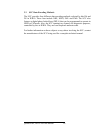
Example 2: Monitoring the status of the transmit and receive buffers in RR0
of Channel A. Register 0 is addressed by default if no register
number is written to WR0
mov dx,base ; load base address
add dx,ContA ; add control reg A offset
in al,dx ; read the status
Quatech Inc., MPA-200/300 Manual 6