


(4/4)
7. Oscillator Circuit
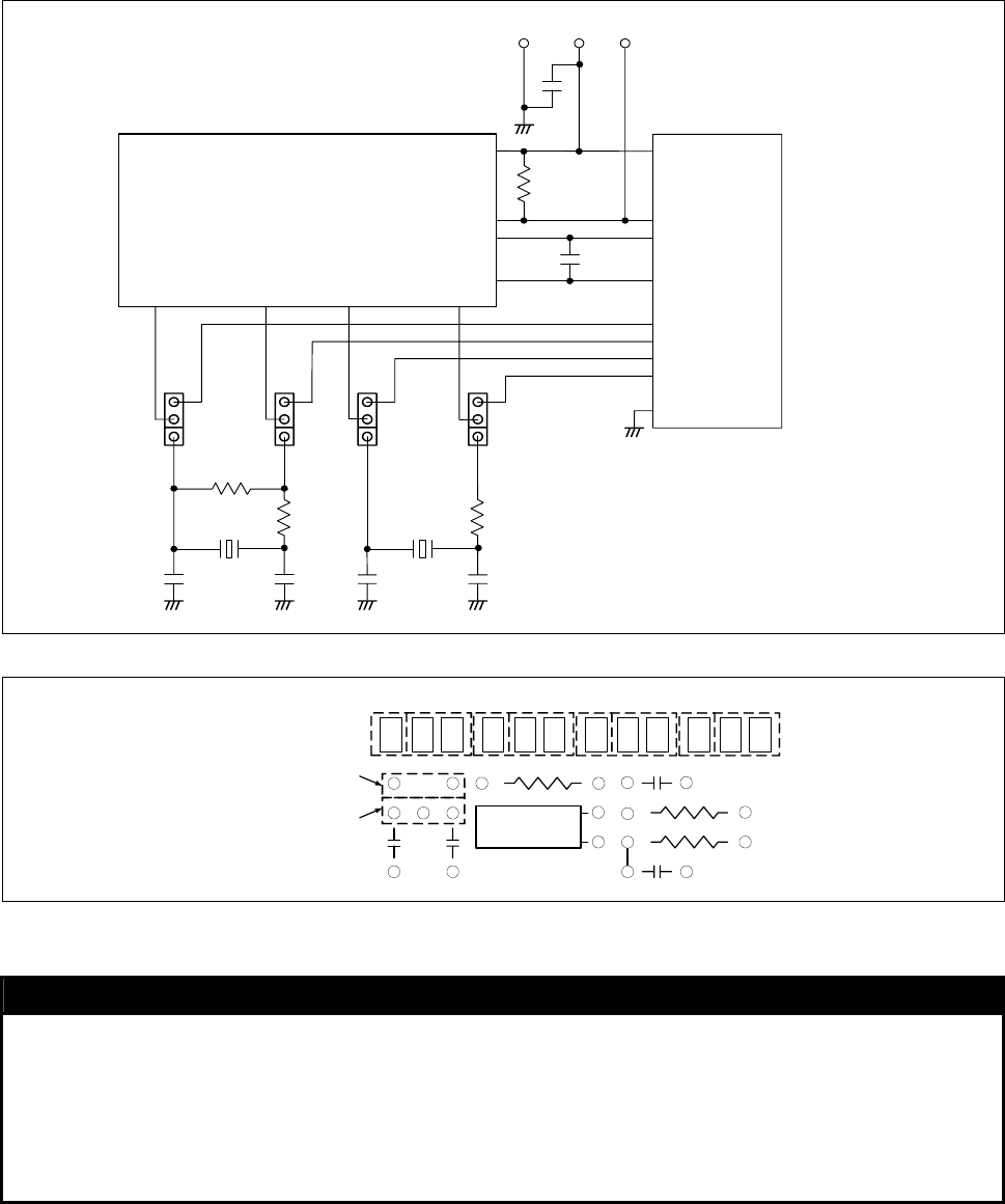
This product has two oscillator circuit patterns for the main clock XIN and sub-clock XCIN. Figures 6 and 7 show the oscillator
circuit diagram and oscillator circuit pattern, respectively. Select one of them according to the oscillator circuitry of the user system.
(1) When using the internal oscillator circuit of the MCU:
The oscillator circuit on the user system may not oscillate because a converter board is used between the emulator MCU and the
user system. In this case, set the jumper switch to INT and mount an oscillator circuit on the M38D29T2-RLFS’s oscillator
circuit pattern. When using the oscillator circuit on the user system, be sure to set the jumper switch to EXT.
(2) When using an oscillator module IC etc. (self-oscillation):
It is not necessary to mount an oscillator circuit on the M38D29T2-RLFS’s oscillator circuit pattern.
XCIN XCOUT XIN XOUT
+
Vref
AVss
RESET*
VCC
CN1-12b(AVss)
CN1-12a( Vref)
CN2-2b(RESET*)
CN2-5b(VCC)
CN1,CN2
CN2-3b(P61/ Xcin)
CN2-3a(P62/ Xcout)
CN2-4b( Xin)
CN2-5a( Xout)
CN2-4a(Vss)
EXT
INT
EXT
INT
EXT
INT
EXT
INT
JP1 JP2JP3 JP4
C1 C 2C3 C4
X1X2
R4
R3
R2
R1
C5
IC1
TP1
RESET
TP2
GND
TP3
VCC
C6
Figure 6 Oscillator circuit diagram
X1
C1 C2
R2
JP2 XOUTJP1 XIN JP3 XCIN JP4 XCOUT
X2
C4
R3
R4
C3
INT EXT INT EXT INT EXT INT EXT
For 3-terminal oscillator
For 2-terminal oscillator
Figure 7 Oscillator circuit pattern
8. Precautions
IMPORTANT
Notes on This Product:
z We cannot accept any request for repair.
z When using the oscillator circuit on the M38D29T2-RLFS, check the output waveform of pins Xout and Xcout by
an oscilloscope.
z When mounting an oscillator circuit on the M38D29T2-RLFS, make sure that 2 mm or more of a DIP pin does not
appear on the rear face (solder side). It may be short-circuited with the DIP pin of the converter board.
z For inquiries about the product or the contents of this manual, contact your local distributor.
Renesas Tools Homepage http://www.renesas.com/tools