CLOCK CIRCUIT S3C8275X/F8275X/C8278X/F8278X/C8274X/F8274X
7-6
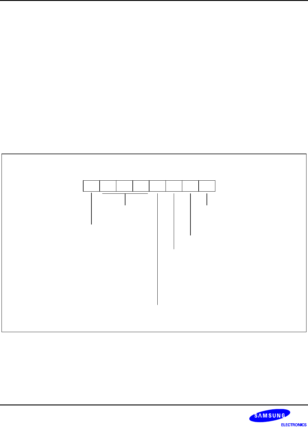
OSCILLATOR CONTROL REGISTER (OSCCON)
The oscillator control register, OSCCON, is located in set 1, bank 0, at address E0H. It is read/write addressable
and has the following functions:
• System clock selection
• Main oscillator control
• Sub oscillator control
• Sub oscillator circuit selection
OSCCON.0 register settings select Main clock or Sub clock as system clock.
After a reset, Main clock is selected for system clock because the reset value of OSCCON.0 is "0".
The main oscillator can be stopped or run by setting OSCCON.3.
The sub oscillator can be stopped or run by setting OSCCON.2.
Oscillator Control Register (OSCCON)
E0H, Set 1, Bank 0, R/W
LSBMSB .7 .6 .5 .4 .3 .2 .1 .0
Not used for S3C8275X/
C8278X/C8274X
System clock selection bit:
0 = Main oscillator select
1 = Sub oscillator select
Sub oscillator control bit:
0 = Sub oscillator RUN
1 = Sub oscillator STOP
Main oscillator control bit:
0 = Main oscillator RUN
1 = Main oscillator STOP
Not used for S3C8275X/C8278X/C8274X
Sub oscillator circuit selection bit:
0 = Initial state
1 = Power saving circuit for sub oscillator
(Automatically cleared to "0" when the sub
oscillator is stopped by OSCCON.2)
NOTES:
1. The OSCCON.7 must be maintained to "1", during
the suboscillator operation.
2. A capacitor (0.1uF) should be connected between
VREG and GND.
Figure 7-10. Oscillator Control Register (OSCCON)


