


19 20
■
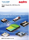
Applications
unit: mm
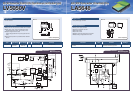
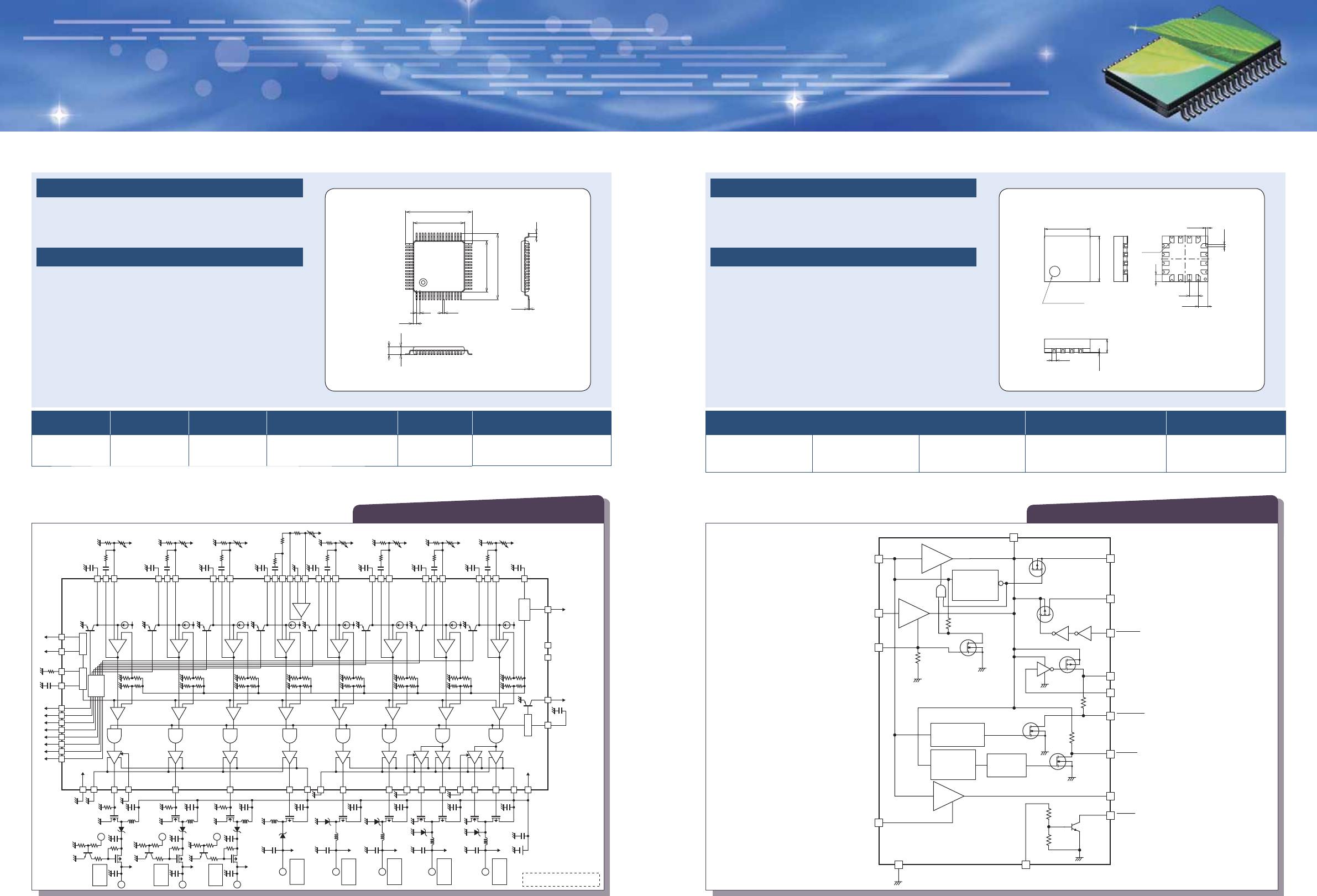
SANYO: TQFP64J(7X7)
8-channel switching regulator control IC
■
Functions/Features
●
Low voltage (3V minimum) operation
●
Reference voltage precision: ± 1%
●
Independent standby function for each of the 8 channels
●
Is capable of driving MOS transistors
●
Synchronous rectifi cation: channels 1 and 2
●
Supports inverting step-up operation
Type Input voltage
Output voltage
Channels
Power stages
Package
Multiple power
supply
3V to 15V
Programmable
externally
8ch (Step up 3, down 5) External TQFP64J(7×7)
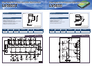
Power Supply ICs for Single Lens Reflex Digital Cameras
Power Supply ICs for Single Lens Reflex Digital Cameras
LV5604T
LV5604T
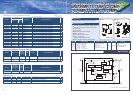
Block Diagram
Pre-output stage
power supply VBIAS1
VBAT
FB1A
Step-down
(DOWN)
V
O
1
3.3V/100mA
V
O
2
3.3V/100mA
OUT1
OUT1N
SYNC1
SYNC1
L: Synchronous
rectification
H: Diode rectification
Signal system
power supply V
CC
+
-
-
VREF
FB1A
IN1
-
FB1
CSOFT1
CTCLK_INCLK_OUT RT
STBY8
STBY7
STBY6
STBY5
STBY4
STBY3
STBY2
STBY1
GND_S
CTL SCP_OUT SCP
(NC) (NC)
SCP
Step-down
(DOWN)
Step-down
(DOWN)
Step-down
(DOWN)
FB2A
OUT2
SYNC2
OUT3
OUT4
OUT2N
+
-
-
FB2A
IN2
-
FB2
CSOFT2
SYNC2
L: Synchronous
rectification
H: Diode rectification
FB3A
+
-
-
FB3A
IN3
-
FB3
CSOFT3
IN4
-
FB4
CSOFT4
V
O
2
3.3V/100mA
FB4A
+
-
-
GND_P(VS1)
VBIAS2
FB4A
IN5
-
RE
IN5
+
RE
FB5RE
IN5
-
FB5
CSOFT5
V
O
3
-4V/100mA
FB5A
FB6A
FB8A
FB7A
Inversion
(INVENT)
IN6
-
FB6
CSOFT6
FB6A
OUT5
+
-
-
FB5A
+
-
IN7
-
FB7
CSOFT7
FB7A
ON/OFF
setting
GND_P(VS2)
OUT8
OUT7
OUT6
SEL_CH8
IN8
-
FB8
CSOFT8
Step-up
(UP)
+
-
-
+
-
-
+
-
-
+
+
-
+
+
-
+
+
-
+
+
-
+
+
-
+
+
-
+
+
-
+
+
-
FB8A
ON/OFF
setting
Step-up
(UP)
ON/OFF
setting
Step-up
(UP)
CTL
CLK
STBY
OSC
SEL_CH8 MODE
Step-down;
Connect to VBIAS
Step-up;
Connect to GND2
Channel 8 step-up/step-down is
selected by SEL_CH8
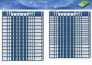
7.0
9.0
7.0
9.0
0.125
0.5
0.16
0.4
(0.5)
(1.0)
1.2max
0.1
1
16
3348
17
64
32
49
■
Applications
unit: mm
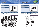
SANYO: VCT16(2.6X2.6)
For digital still cameras
Switching IC between main and backup power supplies
■
Functions/Features
●
Low power dissipation
●
Switching among 3 power sources
(main battery, button battery, external power supply)
●
LDO×3 (2.6V, 3.0V, 3.2V)
●
Three voltage detection circuits (2.6V, 2.8V, 2.2V)
Input voltage Package
Applications
V
CC
1: 2.7V to 4.8V V
CC
2: 3V V
CC
3: 3.5V to 5.2V VCT16(2.6×2.6)
For DSCs and game
machines
Power Supply Switching ICs
Power Supply Switching ICs
LV5621LP
LV5621LP
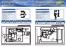
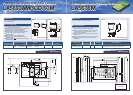
Block Diagram
LDO1
V
OUT
VBATT
BAT_OFF
DC_IN
Lithium-ion/AC adapter
V
IN
(2.7 to 4.8V)
VBOOST
SEL
GND
REG 2.6V
30mA
SW_V
OUT
SW_ON
LDO2
Delay circuit
REG 3.0V
15mA
LDO3
BACK_CNT
DC_IN
VCHG
RESET
PULL_UPV
Pch
VBATT M1
REG 3.2V
60mA
PULL_UPON
Pch
Pch
Nch
Nch
Nch
1.1kΩ
600Ω
10kΩ
200kΩ
22kΩ
22kΩ
Input: LDO2 ON when H
Voltage detection
Set to low at 2.8V
Set to high again at 2.9V
Voltage detection
2.6V
Hysteresis width
40mV
Reset voltage
detection 2.2V
Hysteresis width
0.1V
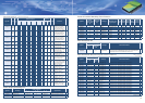
2.6
2.6
0.4
0.8
0.25
(0.035)
SIDE VIEW
SIDE VIEW
BOTTOM VIEW
TOP VIEW
LASER MARKED
INDEX
0.5
(0.55)
(C0.116)
(0.13)
(0.125)
12
16