


Barracuda 180 Product Manual, Rev. A 61
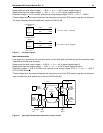
Steady state Low level output voltage* = –.95 V = < V
s
= < –1.55 V (signal negation/logic 0)
Steady state High level output voltage* = –.95 V = < V
s
= < 1.55 V (signal assertion/logic 1)
Differential voltage = +
0.6 V minimum with common-mode voltage ranges 0.700 V = < V
cm
= < 1.800 V.
*These voltages shall be measured between the output terminal and the SCSI device’s logic ground reference.
The output characteristics shall additionally conform to EIA RS-485.
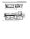
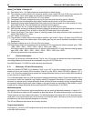
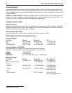
Figure 21. LVD output signals
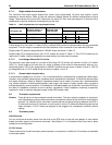
Input characteristics
Each signal (Vs) received by LVD interface receiver circuits shall have the following input characteristics when
measured at the disk drive connector:
Steady state Low level output voltage* = 0.030 V = < V
s
= < 3.6 V (signal negation/logic 0)
Steady state High level output voltage* = –3.6 V = < V
s
= < –0.030 V (signal assertion/logic 1)
Differential voltage = +
0.30 V minimum with common-mode voltage ranges 0.700 V = < V
cm
= < 1.800 V.
(X3T10/1302D Annex A)
*These voltages shall be measured between the output terminal and the SCSI device’s logic ground reference.
Input characteristics shall additionally conform to EIA RS-485-983.
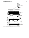
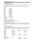
Figure 22. Typical SE-LVD alternative transmitter receiver circuits
Signal +
Signal –
LVD Differential
Driver
1.55V
V
0
= True / Logic 1 / Assertion
–15ma
.95V +15ma
Signal +
Signal –
LVD Differential
Driver
.95V
V
0
= False / Logic 0 / Negation
|V
0
| = .6V
+15ma
1.55V –15ma
VCCA VCCB
Single
Ended
Circuitry
Single
Ended
Receiver
Single
Ended
Negation
Driver
Single
Ended
Assertion
Driver
Single
Ended
Ground
Driver
Single Ended:
LVD:
LVD Signal Drivers
LVD Signal Drivers
LVD
Receiver
Ground
GND
+Signal
–Signal
–Signal