


1 (E)
BKPF-L753A
Table of Contents
Manual Structure
Purpose of this manual ........................................................................................ 3 (E)
Contents ............................................................................................................... 3 (E)
Related manuals................................................................................................... 3 (E)
1. Service Overview
1-1. Notes on Repair Parts ............................................................................1-1 (E)
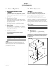
1-2. IC Link Replacement ............................................................................1-1 (E)
1-3. Shield Case (S/N10001 through S/N17325) .........................................1-1 (E)
1-4. Name and Function of Switch/Indicator/etc. ........................................1-2 (E)
1-5. Unleaded Solder ....................................................................................1-3 (E)
2. Electrical Alignment
2-1. Electrical Alignment Overview.............................................................2-1 (E)
2-1-1. Required Equipment and Tools ............................................2-1 (E)
2-1-2. Connection ...........................................................................2-1 (E)
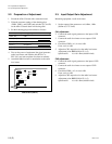
2-2. Preparation of Adjustment ....................................................................2-2 (E)
2-3. Input/Output Gain Adjustment..............................................................2-2 (E)
2-4. CMRR (Common Mode Rejection Ratio) Adjustment.........................2-3 (E)
2-5. Input/Output Gain Adjustment for Customer Setting ...........................2-3 (E)
3. Spare Parts
ADA-55 ..................................................................................................................3-1
CN-1855/1856 ........................................................................................................3-4
DD-36 ..................................................................................................................... 3-4
4. Semiconductor Pin Assignments
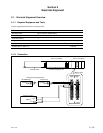
5. Block Diagram
Overall ....................................................................................................................5-1