


— 3 —
TABLE OF CONTENTS
CHAPTER 1. REMOVAL
1-1. Flowchart ......................................................................... 1-1
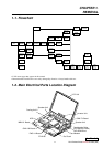
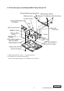
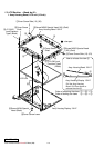
1-2. Main Electrical Parts Location Diagram ......................... 1-1
1-3. Removal ........................................................................... 1-2
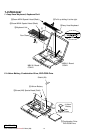
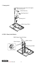
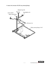
1. Assy Hood Keyboard, Keyboard Unit ............................. 1-2
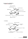
2. Lithium Battery, Combination Drive,
DVD-ROM Drive............................................................. 1-2
3. Combination Drive, DVD-ROM Drive............................ 1-3
1. FXA33/FXA35
/D/FXA36 Model ................................ 1-3
2. FXA32 Model .............................................................. 1-3
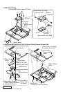
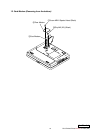
4. HDD, Door Battery.......................................................... 1-4
5. Assy Palmrest, Pad Touch, CNX-129 Board,
Plate Palmrest, Bracket Pad ............................................. 1-4
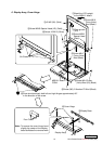
6. Display Assy, Cover Hinge .............................................. 1-5
7. Cooling Unit-2 ................................................................. 1-6
8. PWS-14 Board, Latch Detector ...................................... 1-6
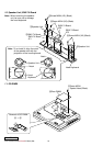
9. PC Card Connector, Card Modem, MBX-61 Board,
Bracket I/O....................................................................... 1-7
10. Speaker Unit, SWX-74 Board ......................................... 1-8
11. SO-DIMM........................................................................ 1-8
12. Card Modem (Removing from the bottom) ..................... 1-9
13. LCD Section – Made by HI – ....................................... 1-10
1. Assy Housing Bezel, LCD unit (15 inch) .................. 1-10
2. Inverter Unit, Harness LCD, FPC,
Assy Housing Display ............................................... 1-11
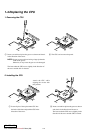
1-4. Replacing the CPU ........................................................1-12
1. Removing the CPU ........................................................ 1-12
2. Installing the CPU.......................................................... 1-12
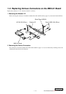
1-5. Replacing Various Connectors on the MBX-61 Board .. 1-13
1. Removing the Bracket I/O ............................................. 1-13
2. Removing the Various Connectors................................. 1-13
1-6. DIP Switch Setting of the MBX-61 Board .................... 1-14
(to 1-14)
Section Title Page
PCG-FXA32/FXA33/FXA35/D/FXA36 (AM)
Confidential
Section Title Page
CHAPTER 2. SELF DIAGNOSTICS ...................... 2-1
(to 2-1)
CHAPTER 3. BLOCK DIAGRAM ............................... 3-1
(to 3-2)
CHAPTER 4. FRAME HARNESS DIAGRAM ........ 4-1
(to 4-2)
CHAPTER 5. EXPLODED VIEWS AND
PARTS LIST............................................ 5-1
5-1. Main Section.................................................................... 5-2
5-1-A FDD Section ............................................................. 5-4(a)
5-2. LCD Section (FXA32/FXA33/FXA36 Model)
– Made by HI – ................................................................ 5-5
5-2-A. LCD Section (FXA35/D Model) – Made by HI – .. 5-6 (a)
5-3. Connector Section............................................................ 5-7
(to 5-8)
History of the changes is shown as the
“Revision History” at the end of this data.