


TA-E1
55
SECTION 3
DIAGRAMS
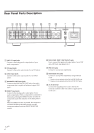
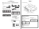
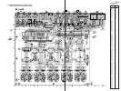
3-1. CIRCUIT BOARDS LOCATION
SECTION 2
ELECTRICAL ADJUSTMENTS
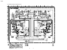
IDLING ADJUSTMENT AND OFFSET VOLTAGE
CHECK
• Perform this adjustment after replacing CP103 and CP104.
• Perform this adjustment more than 10 minutes after supplying
the power.
Connection:
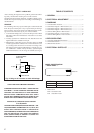
BALANCE OUTPUT LEVEL ADJUSTMENT
• Perform this adjustment when replacing CP102.
• Perform this adjustment after the idling adjustment
Connection:
MAIN board
SW L board
AC J board
LED A board
LED B board
SW P board
PS board
VOL board
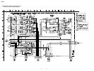
THIS NOTE IS COMMON FOR PRINTED WIRING
BOARDS AND SCHEMATIC DIAGRAMS.
(In addition to this, the necessary note is printed
in each block.)
For schematic diagrams.
Note:
• All capacitors are in µF unless otherwise noted. pF: µµF
50 WV or less are not indicated except for electrolytics
and tantalums.
• All resistors are in Ω and
1
/
4
W or less unless otherwise
specified.
• % : indicates tolerance.
• 2 : nonflammable resistor.
• 5 : fusible resistor.
• C : panel designation.
• S : B+ Line.
• T : B– Line.
• H : adjustment for repair.
• Voltages and waveforms are dc with respect to ground in
playback mode.
• Voltages are taken with a VOM (Input impedance 10 MΩ).
Voltage variations may be noted due to normal produc-
tion tolerances.
• Signal path.
F : TUNER
Note:
The components identi-
fied by mark ! or dotted
line with mark ! are criti-
cal for safety.
Replace only with part
number specified.
Note:
Les composants identifiés par
une marque ! sont critiques
pour la sécurité.
Ne les remplacer que par une
piéce portant le numéro
spécifié.
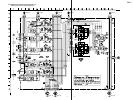
For printed wiring boards.
Note:
• X : parts extracted from the component side.
•
®
: Through hole.
• b : Pattern from the side which enables seeing.
(The other layers' patterns are not indicated.)
Caution:
Pattern face side: Parts on the pattern face side seen from the
(Side B) pattern face are indicated.
Parts face side: Parts on the parts face side seen from the
(Side A) parts face are indicated.
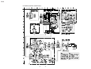
Digital voltmeter
TP501 (L-CH), TP502 (R-CH)
TP503 (L-CH), TP504 (R-CH)
MAIN board
Procedure:
1. Connect the digital voltmeter as shown above.
2. Adjust RV501 (L-CH) and RV502 (R-CH) of the MAIN board
so that the digital voltmeter reads 50 mV ±5 mV. (Idling adjust-
ment)
3. Measure the voltage of both terminals of R221 (L-CH) and R222
(R-CH) of the MAIN board, and check that the voltage is within
2 mV.
(Offset voltage check)
Measuring Adjusting Adjusting
Point Point Value
L-CH TP501 to TP503 RV501 50 mV ± 5 mV
R-CH TP502 to TP504 RV502 50 mV ± 5 mV
Measuring Point Specified Value
L-CH Both terminals of R221 Within 2 mV
R-CH Both terminals of R222 Within 2 mV
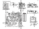
Procedure:
1. Connect as shown above.
2. Rotate the INPUT SELECTOR knob, and set the input source
to LINE 1 .
3. Set the input level so that the oscilloscope waveform level be-
comes approx 3 V.
4. Adjust RV401 (L-CH) and RV402 (R-CH) so that the two wave-
form levels on the oscilloscope become equal and their phases
are reversed.
BALANCED-OUT
2
3
pin
LINE1 input
Set
AF OSC
attenuator
Oscilloscope
Adjusting Value:
Adjusting Point Adjusting Value
L-CH Pin 2 (CH1) and RV401
Pin 3 (CH2) of CN203
R-CH Pin 2 (CH1) and RV401
Pin 3 (CH2) of CN203
Phases of waveforms of
Pins
2
and
3
should be reversed
Waveform of
Pin
2
(CH1)
Waveform of
Pin
3
(CH2)
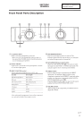
Adjustment Location:
[MAIN board] (Component Side)
OFFSET
VOLTAGE
R222
R221
RV401
BALANCE OUT
LEVEL L CH
RV402
BALANCE OUT
LEVEL R CH
RV501
IDLE
L CH
TP503
RV502
IDLE
R CH
TP501 TP504 TP502