


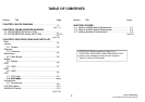

TAB LE O F CO
N
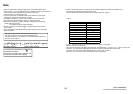
Section Title Page
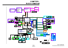
CHAPTER1. BLOCK DIAGRAM……………………………
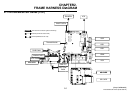
CHAPTER2. FRAME HARNESS DIAGRAM
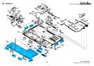
2-1.VPCSA/SB/SC/SD Series (TOP)…………...………………. 2-1
1-1
2-1
(to 1-1)
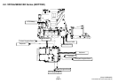
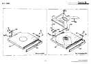
2-2.VPCSA/SB/SC/SD Series (BOTTOM)……………………. 2-2
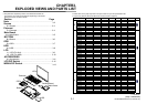
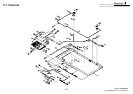
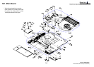
CHAPTER3. EXPLODED VIEWS AND PARTS LIST
Note……………………………………………………………….…
Screws
2-2
3-2
(to 2-2)
Screws
S-1. Screws………………………………………….…….........
Palmrest
P-1. Palmrest………………………………………….......…..…
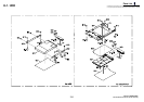
Main Board
M
1
Main
B
oard
3-3
3-4
M
-
1
.
Main
B
oard
………………………………………………
Bottom
B-1. Bottom………………………………………………..………
ODD
D-1. ODD…………………………………………………………
3-5
3-6
3
-
7
HDD
H-1. HDD……………………………………………………………
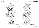
LCD
L-1. LCD (Hot)………………………..................................
L
-
2
LC
D (Mild)
3
7
3-8
3-9
3
10
L
-
2
.
LC
D (Mild)
……………………..................................
Accessories
A-1. Accessories…………………………..…………...…
LCD DIP Switch…………………………………………………
WWAN DIP Switch…………………………………………………
3
-
10
3-11
3-12
3-13
3
(to 3-13)
N
TENTS
Section Title Page
CHAPTER4.OTHERS
4-1. Note for WWAN Board Replacement ……………………
4-2. Note for WIMAX Board Replacement ……………………
4-3. Holding Method of Motherboard……………..……………
4-1
4-2
4-3
(to 4-3)
x SPECIFICATIONS are listed on Page 3-1 of
“CHAPTER3. EXPLODED VIEWS AND PARTS LIST”.
x
History of the changes is shown as the
“
Revision
x
History of the changes is shown as the Revision
History” at the end of this data.
3
[Sony Confidential]
VPCSA/SB/SC/SD Series (9-890-859-XX)