Small Footprint RMII 10/100 Ethernet Transceiver with HP Auto-MDIX Support
Datasheet
Revision 1.0 (05-28-09) 34 SMSC LAN8720/LAN8720i
DATASHEET
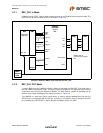
4.12 PHY Address Strapping
The PHY ADDRESS bit is latched into an internal register at the end of a hardware reset. The address
bit is input on the RXER/PHYAD0 pin. The default setting is PHYAD0=0 as described in
Section 5.3.9.1.
4.13 Variable Voltage I/O
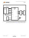
The Digital I/O pins on the LAN8720/LAN8720i are variable voltage to take advantage of low power
savings from shrinking technologies. These pins can operate from a low I/O voltage of +1.8V-10% up
to +3.3V+10%. The I/O voltage the System Designer applies on VDDIO needs to maintain its value
with a tolerance of ± 10%. Varying the voltage up or down, after the transceiver has completed power-
on reset can cause errors in the transceiver operation.
4.14 Transceiver Management Control
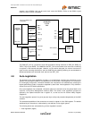
The Management Control module includes 3 blocks:
Serial Management Interface (SMI)
Management Registers Set
Interrupt
4.14.1 Serial Management Interface (SMI)
The Serial Management Interface is used to control the LAN8720/LAN8720i and obtain its status. This
interface supports registers 0 through 6 as required by Clause 22 of the 802.3 standard, as well as
“vendor-specific” registers 16 to 31 allowed by the specification. Non-supported registers (7 to 15) will
be read as hexadecimal “FFFF”.
At the system level there are 2 signals, MDIO and MDC where MDIO is bi-directional open-drain and
MDC is the clock.
A special feature (enabled by register 17 bit 3) forces the transceiver to disregard the PHY-Address in
the SMI packet causing the transceiver to respond to any address. This feature is useful in multi-PHY
applications and in production testing, where the same register can be written in all the transceivers
using a single write transaction.
The MDC signal is an aperiodic clock provided by the station management controller (SMC). The MDIO
signal receives serial data (commands) from the controller SMC, and sends serial data (status) to the
SMC. The minimum time between edges of the MDC is 160 ns. There is no maximum time between
edges.
The minimum cycle time (time between two consecutive rising or two consecutive falling edges) is 400
ns. These modest timing requirements allow this interface to be easily driven by the I/O port of a
microcontroller.
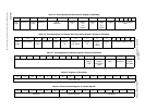
The data on the MDIO line is latched on the rising edge of the MDC. The frame structure and timing
of the data is shown in Figure 4.10 and Figure 4.11.
The timing relationships of the MDIO signals are further described in Section 6.1, "Serial Management
Interface (SMI) Timing," on page 55.


