Ultra Fast USB 2.0 Multi-Slot Flash Media Controller
Datasheet
SMSC USB2250/50i/51/51i 17 Revision 1.1 (05-29-08)
DATASHEET
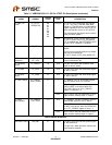
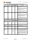
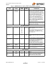
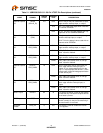
Memory Address
Bus
MA1[1:0] /
CLK_
SEL1[1:0]
25
27
O12 MA[1:0]: These signals address memory
locations within the external memory.
I/O12PD CLK_SEL[1:0]: During nRESET assertion,
these pins will select the operating frequency
of the external clock, and the corresponding
weak pull-down resistors are enabled. When
nRESET is negated, the value on these pins
will be internal latched and these pins will
revert to MA[1:0] functionality; the internal
pull-downs will be disabled.
CLK_SEL[1:0] = '00'. 24MHz
CLK_SEL[1:0] = '01'. RESERVED
CLK_SEL[1:0] = '10'. RESERVED
CLK_SEL[1:0] = '11'. 48MHz
Note: If the latched value is '1', then the
corresponding MA pin is tri-stated
when the chip is in the powerdown
state.
If the latched value is '0', then the
corresponding MA pin will function identically
to the MA[15:3] pins at all times (other than
during nRESET assertion).
Memory Write
Strobe
nMWR 3 O12 Program Memory Write; active low
Memory Read
Strobe
nMRD 115 O12 Program Memory Read; active low
Memory Chip
Enable
nMCE 26 O12 Program Memory Chip Enable; active low.
This signal is asserted when any external
access is being done by the processor.
This signal is held to the logic 'high' while
nRESET is asserted.
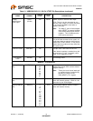
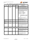
MISC
General Purpose
I/O
LED1 / GPIO1 120 I/O12 GPIO: This pin may be used either as input,
edge sensitive interrupt input, or output.
LED: In addition, as an output, the GPIO1
can be used output controlled by the
LED1_GPIO1 register.
General Purpose
I/O
GPIO3
(VBUS_DET)
121 I/O12 This pin may be used either as input, edge
sensitive interrupt input, or output.
This pin is not 5V tolerant. An external
resistor divider must be used when
connected to VBUS.
Table 5.1 USB2250/50i/51/51i 128-Pin VTQFP Pin Descriptions (continued)
NAME SYMBOL
128-PIN
VTQFP
BUFFER
TYPE DESCRIPTION


