


USB 2.0 High-Speed 3-Port Hub Controller
Datasheet
Revision 1.98 (11-19-07) 16 SMSC USB2513
DATASHEET
3.2 Buffer Type Descriptions
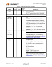
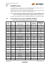
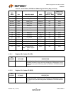
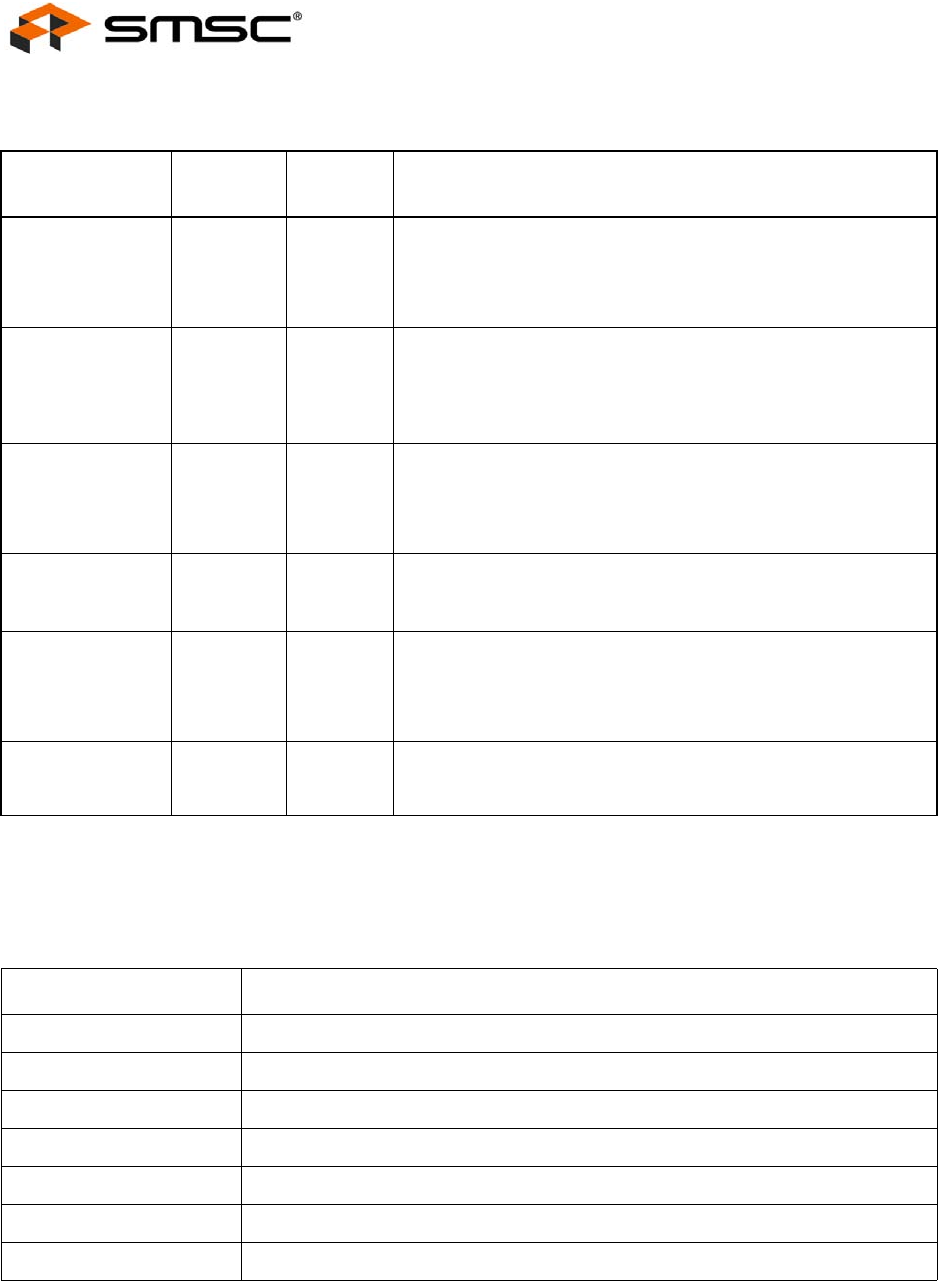
Table 3.3 USB2514 Power, Ground, No Connect
PACKAGE
SYMBOL
36 QFN 48 QFN FUNCTION
VDD18 14 17 VDD Core
+1.8V core power. If the internal regulator is enabled, then this pin
must have a 1.0μF (or greater) ±20% (ESR <0.1Ω) capacitor to
VSS.
VDD33PLL 36 48
VDD 3.3 PLL Regulator Reference
+3.3V power supply for the PLL. If the internal PLL 1.8V regulator
is enabled, then this pin acts as the regulator input.
VDDPLL18 34 46 VDD PLL
+1.8V Filtered analog power for internal PLL. If the internal
regulator is enabled, then this pin must have a 1.0
μF (or greater)
±20% (ESR <0.1Ω) capacitor to VSS.
VDDA33 5
10
29
5
10
41
VDD Analog I/O
+3.3V Filtered analog PHY power, shared between adjacent ports.
VDD33/VDD33CR 23
15
30
18
VDDIO/VDD 3.3 Core Regulator Reference
+3.3V power supply for the Digital I/O
If the internal core regulator is enabled, then VDD33CR acts as
the regulator input.
VSS n/a n/a VSS
Ground
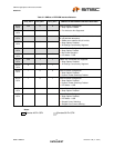
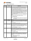
Table 3.4 USB2514 Buffer Type Descriptions
BUFFER DESCRIPTION
I Input.
IPD Input with internal weak pull-down resistor.
IPU Input with internal weak pull-up resistor.
IS Input with Schmitt trigger.
O12 Output 12mA.
OD12 Open drain... 12mA sink.
I/O12 Input/Output buffer with 12mA sink and 12mA source.