


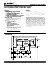
7
S93WD462/S93WD463
2029 2.2 1/23/01SUMMIT MICROELECTRONICS, Inc.
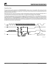
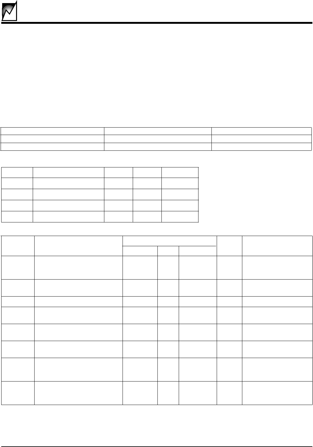
ABSOLUTE MAXIMUM RATINGS*
Temperature Under Bias ....................................................................................................................................–55°C to +125°C
Storage Temperature .........................................................................................................................................–65°C to +150°C
Voltage on any Pin with Respect to Ground
(1)
............................................................................................. –2.0V to +V
CC
+2.0V
V
CC
with Respect to Ground .................................................................................................................................. –2.0V to +7.0V
Package Power Dissipation Capability (Ta = 25°C) ............................................................................................................. 1.0W
Lead Soldering Temperature (10 secs) .............................................................................................................................. 300°C
Output Short Circuit Current
(2)
........................................................................................................................................... 100 mA
*COMMENT
Stresses above those listed under “Absolute Maximum Ratings” may cause permanent damage to the device. These are stress ratings only, and functional
operation of the device at these or any other conditions outside of those listed in the operational sections of this specification is not implied. Exposure to
any absolute maximum rating for extended periods may affect device performance and reliability.
Note:
(1) The minimum DC input voltage is –0.5V. During transitions, inputs may undershoot to –2.0V for periods of less than 20 ns. Maximum DC
voltage on output pins is V
CC
+0.5V, which may overshoot to V
CC
+2.0V for periods of less than 20 ns.
(2) Output shorted for no more than one second. No more than one output shorted at a time.
(3) This parameter is tested initially and after a design or process change that affects the parameter.
(4) Latch-up protection is provided for stresses up to 100 mA on address and data pins from –1V to V
CC
+1V.
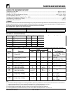
D.C. OPERATING CHARACTERISTICS (over recommended operating conditions unless otherwise specified)
Limits
Symbol Parameter Min. Typ. Max. Units Test Conditions
I
CC
Power Supply Current 3 mA DI = 0.0V, f
SK
= 1MHz
(Operating) V
CC
= 5.0V, CS = 5.0V,
Output Open
I
SB
Power Supply Current 50 µA CS = 0V
(Standby) Reset Outputs Open
I
LI
Input Leakage Current 2 µA V
IN
= 0V to V
CC
I
LO
Output Leakage Current 10 µA V
OUT
= 0V to V
CC
,
(Including ORG pin) CS = 0V
V
IL1
Input Low Voltage -0.1 0.8 V 4.5V-V
CC
<5.5V
V
IH1
Input High Voltage 2 V
CC
+1 V
V
IL2
Input Low Voltage 0 V
CC
X0.2 V 1.8V-V
CC
<2.7V
V
IH2
Input High Voltage V
CC
X0.7 V
CC
+1 V
V
OL1
Output Low Voltage 0.4 V 4.5V-V
CC
<5.5V
V
OH1
Output High Voltage 2.4 V I
OL
= 2.1mA
I
OH
= -400µA
V
OL2
Output Low Voltage 0.2 V 1.8V-V
CC
<2.7V
V
OH2
Output High Voltage V
CC
-0.2 V I
OL
= 1mA
I
OH
= -100µA
2029 PGM T3.0
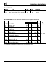
RELIABILITY CHARACTERISTICS
Symbol Parameter Min. Max. Units Reference Test Method
N
END
(3)
Endurance 100,000 Cycles/Byte MIL-STD-883, Test Method 1033
T
DR
(3)
Data Retention 100 Years MIL-STD-883, Test Method 1008
V
ZAP
(3)
ESD Susceptibility 2000 Volts MIL-STD-883, Test Method 3015
I
LTH
(3)(4)
Latch-Up 100 mA JEDEC Standard 17
2029 PGM T2.1
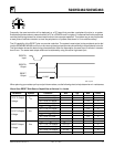
Temperature Min Max
Commercial 0°C +70°C
Industrial -40°C +85°C
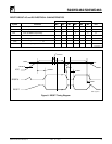
RECOMMENDED OPERATING CONDITIONS
2029 PGM T7.0