(1/2)
001-02 / 20080116 / e721_dea252450bt_7012.fm
• All specifications are subject to change without notice.
Multilayer Chip Band Pass Filters(Balance Output Type)
For Bluetooth & 2.4GHz W-LAN
DEA Series DEA252450BT-7012D1
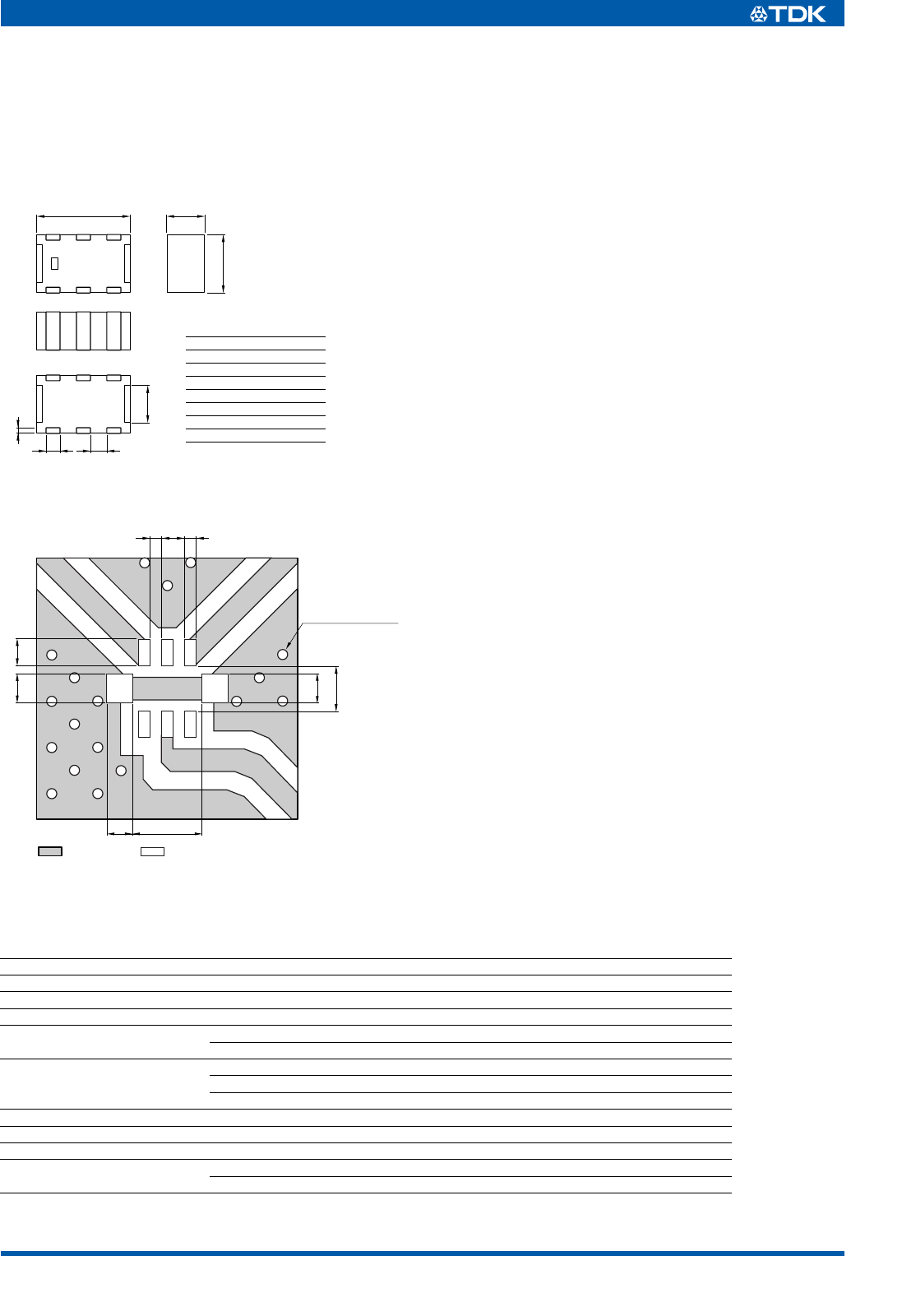
SHAPES AND DIMENSIONS
RECOMMENDED PC BOARD PATTERNS
ELECTRICAL CHARACTERISTICS
Item Typical value
Frequency range (Pass band) 2400 to 2500MHz —
Unbalanced impedance 50Ω(Nominal) —
Balanced impedance 100Ω(Nominal) —
Insertion loss
[+25°C] 1.9dB max. 1.5dB
[–40 to +85°C] 2.2dB max. —
Attenuation
[880 to 960MHz] 40dB min. 50dB
[1710 to 1910MHz] 32dB min. 42dB
[4800 to 5000MHz] 30dB min. 40dB
Unbalanced port return loss 10dB min. 14dB
Phase difference at balanced port 180±12deg 188deg
Amplitude imbalance at balanced port 0±1.0dB 0dB
Temperature range
Operating –40 to +85°C
Storage –40 to +85°C
Conformity to RoHS Directive
1.0max.
2.0±0.2
1.3±0.3
0.4±0.15 0.3±0.1
2.5±0.2
765
48
123
Dimensions in mm
0.2±0.15
1 N.C.
2 Unbalanced
3 DC feed or N.C.
4 GND
5 Balanced
6 N.C.
7 Balanced
8 GND
Terminal functions
Line width be designed to mach 50Ω characteristic impedance
depending on PCB material and thickness
Land
Solder resist
2.10.8
0.9
1.4
0.80.9
0.35 0.35
Dimensions in mm
ø0.3 Through-hole
• Conformity to RoHS Directive: This means that, in conformity with EU Directive 2002/95/EC, lead, cadmium, mercury, hexavalent chromium, and
specific bromine-based flame retardants, PBB and PBDE, have not been used, except for exempted applications.


