


9–1
WFM 300A
Section 9
Diagrams/Circuit Board Illustrations
Symbols
Graphic symbols and class designation letters are based on ANSI Standard Y32.2–1975.
Logic symbology is based on ANSI Y32.14–1973 in terms of positive logic. Logic
symbols depict the logic function performed and may differ from the manufacturer’s data.
Overline, parenthesis, or leading slash indicate a low asserting state.
Example: ID CONTROL, (ID CONTROL), or /ID CONTROL.
Abbreviations are based on ANSI Y1.1–1972.
Other ANSI standards that are used in the preparation of diagrams by Tektronix, Inc. are:
Y14.15, 1966 -- Drafting Practices.
Y14.2, 1973 -- Line Conventions and Lettering.
Y10.5, 1968 -- Letter Symbols for Quantities Used in Electrical Science and
Electrical Engineering.
American National Standard Institute
1430 Broadway, New York, New York 10018
Component Values
Electrical components shown on the diagrams are in the following units unless noted
otherwise:
Capacitors: Values one or greater are in picofarads (pF).
Values less than one are in microfarads (mF).
Resistors = Ohms (W).
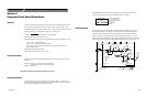
The following information and special symbols may appear in this manual.
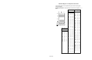
Assembly Numbers
Each assembly in the instrument is assigned an assembly number (e.g., A20). The
assembly number appears on the diagram (in circuit board outline), circuit board illustra-
tion title, and lookup table for the schematic diagram.
The Replaceable Electrical Parts List is arranged by assembly number in numerical
sequence; the components are listed by component number. Example:
Chassis–mounted components
have no Assembly No. prefix.
See end of Replaceable Electrical
Parts List
Assembly
Number
Component Number
A23 A2 R1234
Subassembly
Number (if used)
Schematic Circuit
Number
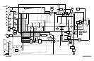
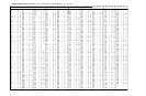
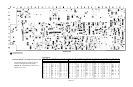
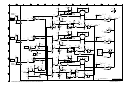
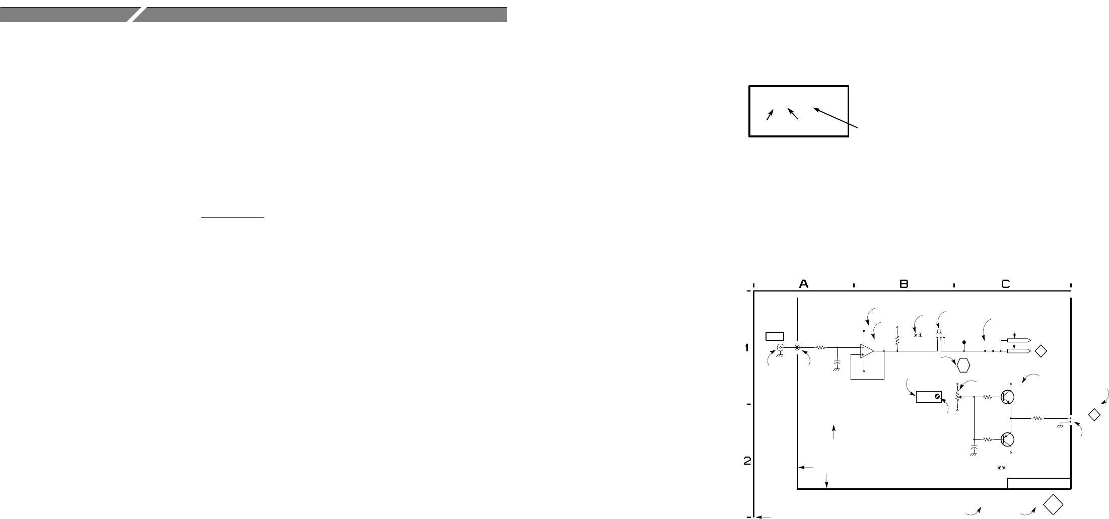
Grid Coordinates
The schematic diagram and circuit board component location illustration have grids. A
lookup table with the grid coordinates is provided for ease of locating the component.
Only the components illustrated on the facing diagram are listed in the lookup table.
When more than one schematic diagram is used to illustrate the circuitry on a circuit
board, the circuit board illustration will only appear opposite the first diagram; the lookup
table will list the diagram number of other diagrams that the other circuitry appears on.
WIRE STRAP
MODULE
PLUG
P1
NEGATIVE
PORTS
IC TYPE
CHANGED
PART
+12V
DECOUPLED OR
FILTERED VOLTAGE
R500
20K
+12V3
REAR
PANEL
INPUT
BNC
J1
(FEMALE)
PAD
FRONT PANEL
NOMENCLATURE
C1
10UF
2
3
6
7
4
U1
741
-12V
R5
1.0
NC
ROTATE
H
HEAT SINK
2
REFER TO
WAVEFORM
123
J1
R4
20K
Q8
W4
0 OHM
+11.8V +15V
-11.8V
TP1
/VIDEO
(VIDEO)
R55
100.0
CLOCKWISE
AJUSTMENT
1
2
J3
12
W751
A3
ANALOG
BOARD
SCHEMATIC &
BOARD REF
PART NAME,
2
R100
R85
SEL
SEE PARTS LIST
FOR SELECTION
CRITERIA
SQUARE PIN
CONNECTOR
PART OF A1 MAIN BOARD
R56
100.0
Q6
-15V
SEE PARTS LIST FOR
EARLIER VALUES AND
SERIAL NUMBER RANGES.
C27
0.1UF
SCREWDRIVER
ADJUSTMENT
CIRCUIT BOARD
OUTLINE
& SNUBBER
BASE DRIVE
TITLE
FUNCTION BLOCK
INSTRUMENT NAME
SCHEMATIC NAME & NUMBER ASSEMBLY NUMBER
VERTICAL INPUT
1
A1
COMPONENT LOCATOR GRID