


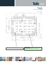
GE863-QUAD
GE863-PY
1vv0300715 Rev. 1 - 19/09/06
Reproduction forbidden without Telit Communications S.p.A. written authorization - All Right reserved page 70 of 79
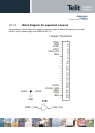
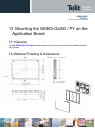
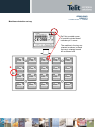
13.2.2 Debug of the GE863 in Production
To test and debug the mounting of the GE863, we strongly recommend to foreseen test pads on the
host PCB, in order to check the connection between the GE863 itself and the application and to test
the performance of the module connecting it with an external computer. Depending by the customer
application, these pads include, but are not limited to the following signals:
• TXD
• RXD
• ON/OFF
• RESET
• GND
• VBATT
• TX_TRACE
• RX_TRACE
• PWR_CTL
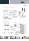
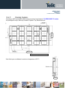
13.2.3 Stencil
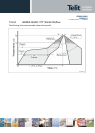
Stencil’s apertures layout can be the same of the recommended footprint (1:1), we suggest a
thickness of stencil foil ≥ 120µm.
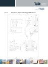
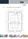
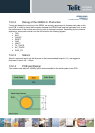
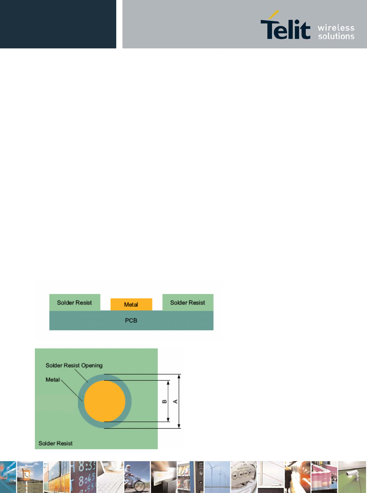
13.2.4 PCB pad Design
“Non solder mask defined” (NSMD) type is recommended for the solder pads on the PCB.