SLUU186 − March 2004
6
TPS40055-Based Design Converts 12-V Bus to 1.8 V at 15 A (HPA070)
4 Component Selection
4.1 TPS40055 Device Selection
The TPS4005x family of parts offers a range of output current configurations including source only (TPS40054),
source/sink (TPS40055), or source/sink with V
OUT
prebias (TPS40057). In this converter the TPS40055 with
source/sink capability is selected. This serves to maintain continuous inductor ripple current all the way to zero
load to improve the small signal loop response by preventing the inductor current from transitioning to the
discontinuous current mode.
The TPS4005x family is packaged in TI’s PWP PowerPAD thermally enhanced package which should be
soldered to the PCB using standard solder flow techniques. The PowerPAD technology uses a thermally
conductive epoxy to attach the integrated circuit die to the leadframe die pad, which is exposed on the bottom
of the completed package. The PWP PowerPAD package has a θ
JC
= 2°C/W which helps keep the junction
temperature rise relatively low even with the power dissipation inherent in the onboard MOSFET drivers. This
power loss is proportional to switching frequency, drive voltage, and the gate charge needed to enhance the
N-channel MOSFETs. Effective heat removal allows the use of ultra-small packaging while maintaining high
component reliability.
The technical brief, PowerPAD Thermally Enhanced Package
[2]
contains more information on the PowerPAD
package.
4.2 Frequency of Operation
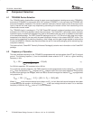
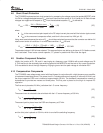
The clock oscillator frequency for the TPS40055 is programmed with a single resistor from RT (pin 2) to signal
ground. The following equation (1) from the datasheet allows selection of RT in kΩ for a given switching
frequency in kHz.
R
T
+ R2 +
1
f
SW
17.82 10
*6
* 23 (kW)
For 300-kHz operation, R2 is selected to be 165 kΩ.
For a particular operating frequency, the PWM ramp time must be programmed via the resistor R
KFF
connected
to V
IN
. Also, the selection of R
KFF
programs the V
IN
voltage at which the circuit starts operation. This prevents
the circuit from starting at low voltages, which can lead to current flow larger than desired. R
KFF
is programmed
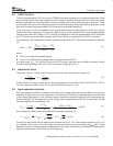
using equation (2).
R
KFF
+ R6 +
ǒ
V
IN(min)
* 3.5
Ǔ
ǒ
58.14 R
T
) 1340
Ǔ
(
kW
)
Where V
IN(min)
is the minimum startup input voltage, and R
T
is in kΩ. Note that internal tolerances have been
incorporated into this equation, so the actual V
IN(min)
of the input voltage should be used. For an oscillator
frequency of 300-kHz, the R
KFF
value of 71.5 kΩ is selected.
(1)
(2)


