


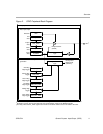
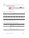

Registers
15General-Purpose Input/Output (GPIO)SPRU724
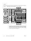
5 Registers
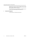
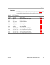
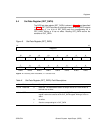
The GPIO peripheral is configured through the registers listed in Table 2. See
the device-specific datasheet for the memory address of these registers.
Table 2. GPIO Registers
Offsets Acronym Register Name Section
0008 BINTEN Interrupt Per-Bank Enable Register 5.1
0010 DIR Direction Register 5.2
0014 OUT_DATA Output Data Register 5.3
0018 SET_DATA Set Data Register 5.4
001C CLR_DATA Clear Data Register 5.5
0020 IN_DATA Input Data Register 5.6
0024 SET_RIS_TRIG Set Rising Edge Interrupt Register 5.7
0028 CLR_RIS_TRIG Clear Rising Edge Interrupt Register 5.8
002C SET_FAL_TRIG Set Falling Edge Interrupt Register 5.8
0030 CLR_FAL_TRIG Clear Falling Edge Interrupt Register 5.9