DM9161B
10/100 Mbps Fast Ethernet Physical Layer Single Chip Transceiver
Final 6
Version: DM9161B-12-DS-F01
January 31, 2008
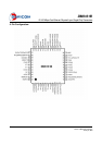
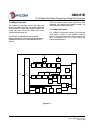
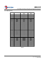
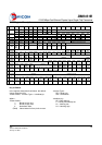
5. Pin Description
I: Input, O: Output, LI: Latch input when power-up/reset, Z: Tri-State output, U: Pulled high D: Pulled low
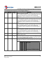
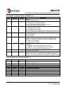
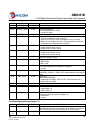
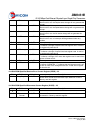
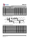
5.1 Normal MII Interface, 21 pins
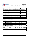
Pin No.
Pin Name
I/O
Description
16 TXER/TXD [4]
I Transmit Error/The Fifth TXD Data Bit
In 100Mbps mode, when the signal indicates active high and TXEN is
active, the HALT symbol substitutes the actual data nibble.
In 10Mbps, the input is ignored
In bypass mode (bypass BP4B5B), TXER becomes the TXD [4] pin, the
fifth TXD data bit of the 5B symbol
20,19,18,17 TXD [0:3] I Transmit Data
4-bit nibble data inputs (synchronous to the TXCLK) when in 10/100Mbps
nibble mode.
In 10Mbps GPSI (7-Wired) mode, the TXD [0] pin is used as the serial
data input pin, and TXD [1:3] are ignored.
21 TXEN I Transmit Enable
Active high indicates the presence of valid nibble data on the TXD [0:3] for
both 100Mbps and 10Mbps nibble modes.
In 10Mbps GPSI (7-Wired) mode, active high indicates the presence of
valid 10Mbps data on TXD [0].
22 TXCLK/
ISOLATE
O,
Z,
LI
(D)
Transmit Clock
The transmitting clock provides the timing reference for the transfer of the
TXEN, TXD, and TXER. TXCLK is provided by the PHY
25MHz in 100Mbps nibble mode, 2.5MHz in 10Mbps nibble mode, 10MHz
in 10Mbps GPSI (7-Wired) mode
ISOLATE Setting: (When power up reset, latch input)
0: Reg 0.10 will be initialized to “0”. (Ref.to 8.1 Basic Control Register)
1: Reg 0.10 will be initialized to “1”.
24 MDC I Management Data Clock
Synchronous clock for the MDIO management data. This clock is
provided by management entity, and it is up to 2.5MHz
25 MDIO I/O Management Data I/O
Bi-directional management data which may be provided by the station
management entity or the PHY
29,28,27,26 RXD[0:3]
/PHYAD[0:3]
O,
Z,
LI
(D)
Receive Data Output
4-bit nibble data outputs (synchronous to RXCLK) when in 10/100Mbps
MII mode
In 10Mbps GPSI (7-Wired) mode, the RXD [0] pin is used as the serial
data output pin, and the RXD [1:3] are ignored
PHY address [0:3] (power up reset latch input)
PHY address sensing input pins
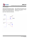
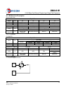
32 MDINTR IO,
LI
(D)
Status Interrupt Output:
Whenever there is a status change (link, speed, duplex depend on
interrupt register [21] )
The interrupt output assert low when pull up.
Asserted high when pull down.