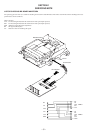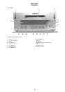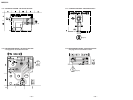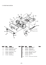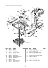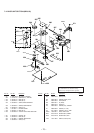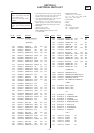
MDS-SD1
– 37 – – 38 –
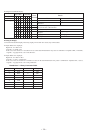
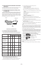
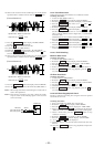
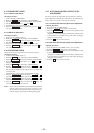
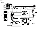
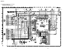
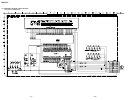
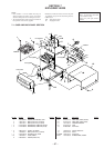
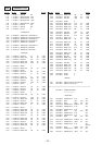
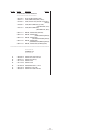
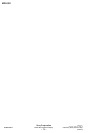
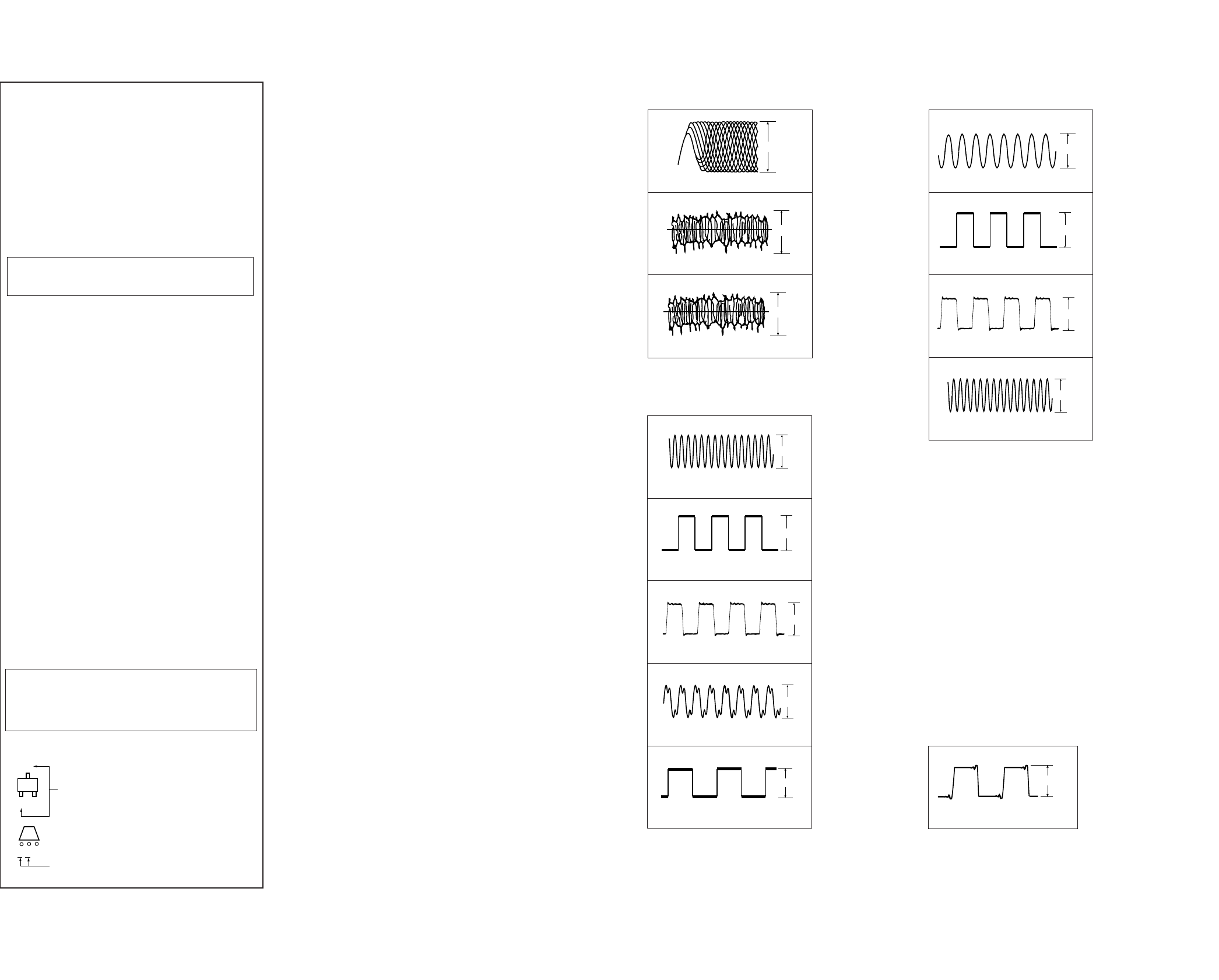
WAVEFORMS
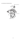
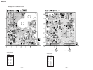
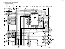
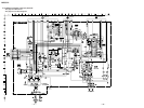
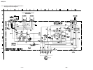
– BD (1/2) SECTION –
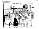
– MAIN SECTION –
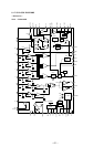
THIS NOTE IS COMMON FOR PRINTED WIRING
BOARDS AND SCHEMATIC DIAGRAMS.
(In addition to this, the necessary note is printed
in each block.)
For schematic diagrams.
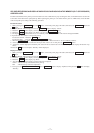
Note:
• All capacitors are in µF unless otherwise noted. pF: µµF
50 WV or less are not indicated except for electrolytics
and tantalums.
• All resistors are in Ω and
1
/
4
W or less unless otherwise
specified.
•
¢
: internal component.
• C : panel designation.
For printed wiring boards.
Note:
• X : parts extracted from the component side.
• Y : parts extracted from the conductor side.
• p : parts mounted on the conductor side.
•
®
: Through hole.
• b : Pattern from the side which enables seeing.
(The other layers' patterns are not indicated.)
• U : B+ Line.
• V : B– Line.
• H : adjustment for repair.
• no mark : STOP
( ) : Play the test disc (TDYS-1)
< > : REC
∗
: Can not be measured.
• Voltages are taken with a VOM (Input impedance 10 MΩ).
Voltage variations may be noted due to normal produc-
tion tolerances.
• Waveforms are taken with a oscilloscope.
Voltage variations may be noted due to normal produc-
tion tolerances.
• Circled numbers refer to waveforms.
• Signal path.
E : PB
q : REC
a : PB (DIGITAL OUT)
r : REC (DIGITAL IN)
• Abbreviation
HK : Hong Kong model.
SP : Singapore model.
Note: The components identified by mark ! or dotted line
with mark ! are critical for safety.
Replace only with part number specified.
• Indication of transistor
C
These are omitted
EB
Caution:
Pattern face side: Parts on the pattern face side seen from the
(Side B) pattern face are indicated.
Parts face side: Parts on the parts face side seen from the
(Side A) parts face are indicated.
Q
C
These are omitte
EB
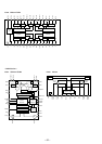
1
IC901 %• (OSCO)
1
2
3
4
5
6
7
8
IC101 1, 2 (I, J) (PLAY mode)
IC101 4 (A) (PLAY mode)
IC101 8, 9 (E, F) (PLAY mode)
IC121 !§ (OSCI)
IC121 @¶ (LRCK)
IC121 @ª (FS256)
IC121 @• (XBCK)
IC121 (º (FS4)
IC201 !¶ (LRCK1)
IC201 !§ (BCK)
IC201 !™ (SYSCLK)
IC701 !£ (XOUT)
1
2
3
4
0.06Vp-p
3.8Vp-p
2.822MHz
3.2Vp-p
10MHz
3.8Vp-p
44.1kHz
3.4Vp-p
2.822MHz
3.0Vp-p
22.581MHz
3.9Vp-p
2.4MHz
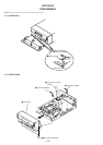
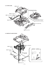
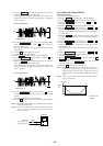
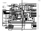
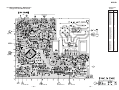
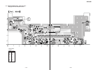
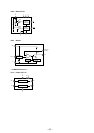
– BD (1/2) SECTION –
– DISPLAY SECTION –