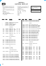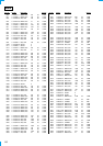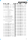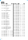
MDX-C6500RV
2121
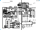
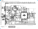
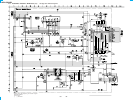
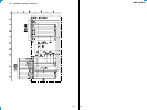
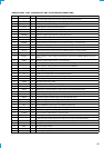
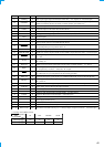
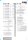
4-5. NOTE FOR PRINTED WIRING BOARDS AND SCHEMATIC DIAGRAMS
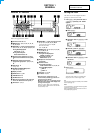
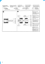
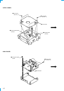
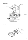
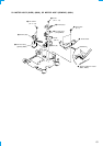
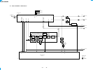
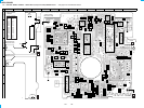
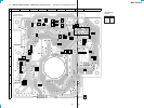
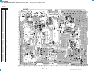
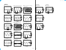
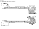
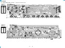
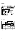
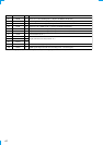
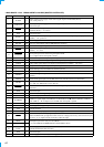
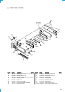
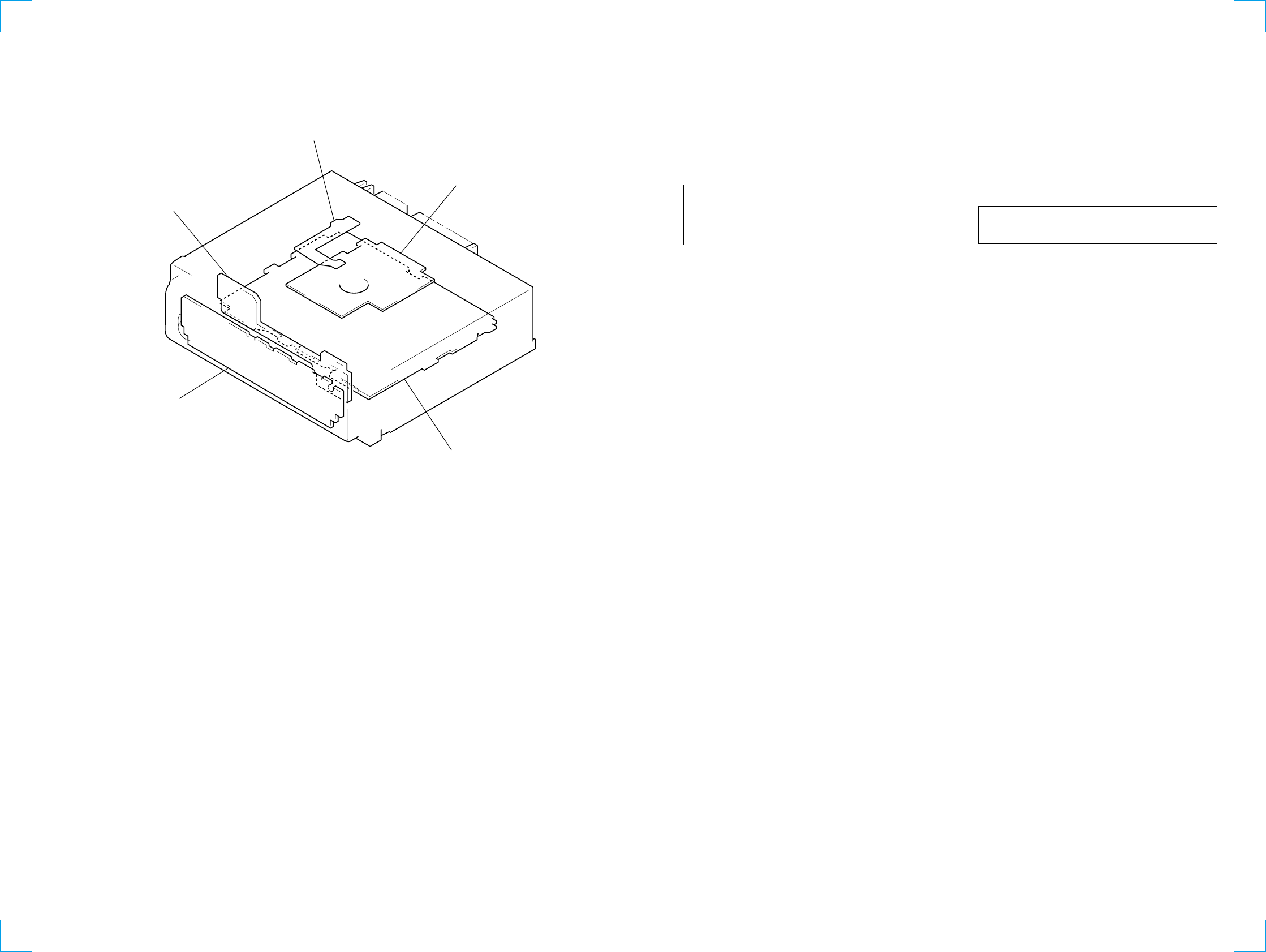
SUB board
SENSOR board
SERVO board
MAIN board
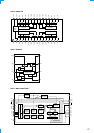
KEY board
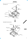
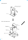
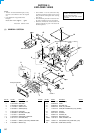
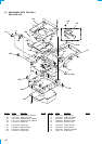
• Circuit Boards Location
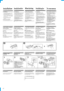
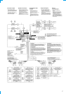
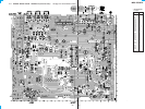
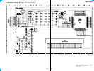
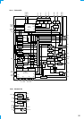
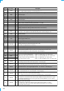
Note on Printed Wiring Board:
• X : parts extracted from the component side.
• Y : parts extracted from the conductor side.
•
z
: Through hole.
•
f
: internal component.
• b : Pattern from the side which enables seeing.
(The other layers' patterns are not indicated.)
Caution:
Pattern face side: Parts on the pattern face side seen from
(Conductor Side) the pattern face are indicated.
Parts face side: Parts on the parts face side seen from
(Component Side) the parts face are indicated.
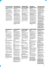
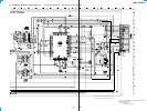
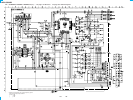
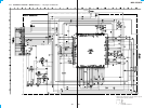
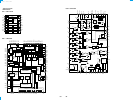
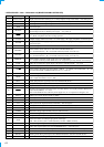
Note on Schematic Diagram:
• All capacitors are in µF unless otherwise noted. pF: µµF
50 WV or less are not indicated except for electrolytics
and tantalums.
• All resistors are in Ω and
1
/
4
W or less unless otherwise
specified.
• % : indicates tolerance.
•
f
: internal component.
• C : panel designation.
• U : B+ Line.
• Power voltage is dc 14.4V and fed with regulated dc power
supply from ACC and BATT cords.
• Voltages are taken with a VOM (Input impedance 10 MΩ).
Voltage variations may be noted due to normal produc-
tion tolerances.
• Waveforms are taken with a oscilloscope.
Voltage variations may be noted due to normal produc-
tion tolerances.
• Circled numbers refer to waveforms.
• Signal path.
E : MD PLAY
F : FM
f : MW/LW
L : BUS AUDIO IN
Note: The components identified by mark 0 or dotted line
with mark 0 are critical for safety.
Replace only with part number specified.