


Chapter 4 133
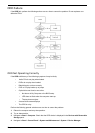
Post Codes
These tables describe the POST codes and descriptions during the POST.
Sec: NO_EVICTION_MODE_DEBUG EQU 1 (CommonPlatform\sec\Ia32\SecCore.inc)
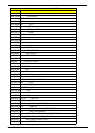
Code Description
0xC2 MTRR setup
0xC3 Enab le cache
0xC4 Est ablish cache tags
0xC5 Enter NEM, Place the BSP in No Fill mode, set CR0.CD = 1, CR0.NW = 0.
0xCF Cach e Init Finished
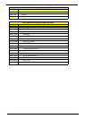
Memory:
DEBUG_BIOS equ 1 (Chipset\Alviso\MemoryInitAsm\IA32\IMEMORY.INC)
Code Description
0xA0 First memory check point
0x01 En able MCHBAR
0x02 Check for DRAM initialization interrupt and reset fail
0x03 Verify all DIMMs are DDR or DDR2 and unbuffered
0x04 Detect an improper warm reset and handle
0x05 Detect if ECC SO-DIMMs are present in the system
0x06 Verify all DIMMs are single or double sided and not asymmetric
0x07 Verify all DIMMs are x8 or x16 width
0x08 Find a common CAS latency between the DIMMS and the MCH
0x09 Determine the memory frequency and CAS latency to program
0x10 Determine the smallest common TRAS for all DIMMs
0x11 Determine the smallest common TRP for all DIMMs
0x12 Determine the smallest common TRCD for all DIMMs
0x13 Determine the smallest refresh period for all DIMMs
0x14 Verify burst length of 8 is supported by all DIMMs
0x15 Determine the smallest tWR supported by all DIMMs
0x16 Determine DIMM size parameters
0x17 Program the correct system memory frequency
0x18 Determine and set the mode of operation for the memory channels
0x19 Program clock crossing registers
0x20 Disable Fast Dispatch
0x21 Program the DRAM Row Attributes and DRAM Row Boundary registers
0x22 Program the DRAM Bank Architecture register
0x23 Program the DRAM Timing & and DRAM Control registers
0x24 Prog ram ODT
0x25 Pe rform steps required before memory init
0x26 Program the receive enable reference timing control register
Program the DLL Timing Control Registers , RCOMP settings
0x27 Enable DRAM Channel I/O Buffers
0x28 Enable all clocks on populated rows