


Chapter 4 147
POST Codes Tables
These tables describe the chipset and core POST codes, functions, phases, and components for the POST.
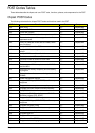
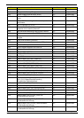
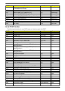
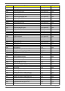
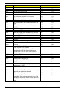
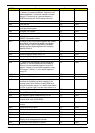
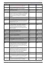
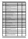
Chipset POST Codes
The following table details the chipset POST codes and functions used in the POST.
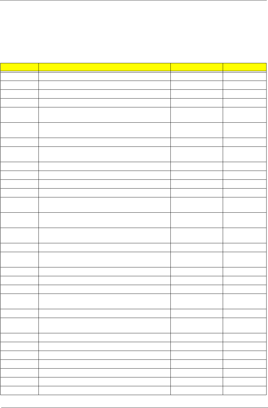
POST Code Function Phase Component
0xA0 MRC Entry PEI chipset/MRC
0x01 Enable MCHBAR PEI chipset/MRC
0x02 Check ME existence PEI chipset/MRC
0x03 Check for DRAM initialization interrupt and reset fail PEI chipset/MRC
0x04 Determine the system Memory type based on first
populated socket
PEI chipset/MRC
0x05 Verify all DIMMs are DDR2 and SO-DIMMS, which
are unbuffered
PEI chipset/MRC
0x06 Verify all DIMMs are Non-ECC PEI chipset/MRC
0x07 Verify all DIMMs are single or double sided and not
mixed
PEI chipset/MRC
0x08 Verify all DIMMs are x8 or x16 width PEI chipset/MRC
0x09 Calculate number of Row and Column bits PEI chipset/MRC
0x10 Calculate number of banks for each DIMM PEI chipset/MRC
0x11 Determine raw card type PEI chipset/MRC
0x12 Find a common CAS latency between the DIMMS
and the MCH
PEI chipset/MRC
0x13 Determine the memory frequency and CAS latency
to program
PEI chipset/MRC
0x14 Determine the smallest common timing value for all
DIMMS
PEI chipset/MRC
0x17 Power management resume PEI chipset/MRC
0x18 Program DRAM type (DDR2/DDR3) and Power up
sequence
PEI chipset/MRC
0x19 Program the correct system memory frequency PEI chipset/MRC
0x20 Program the correct Graphics memory frequency PEI chipset/MRC
0x21 Early DRC initialization PEI chipset/MRC
0x22 Program the DRAM Row Attributes and DRAM Row
Boundary registers PRE JEDEC.
PEI chipset/MRC
0x23 Program the RCOMP SRAM registers PEI chipset/MRC
0x24 Program DRAM type (DDR2/DDR3) and Power up
sequence
PEI chipset/MRC
0x25 Program the DRAM Timing PEI chipset/MRC
0x26 Program the DRAM Bank Architecture register PEI chipset/MRC
0x27 Enable all clocks on populated rows PEI chipset/MRC
0x28 Program MCH ODT PEI chipset/MRC
0x29 Program tRD PEI chipset/MRC
0x30 Miscellaneous Pre JEDEC steps PEI chipset/MRC
0x31 Program clock crossing registers PEI chipset/MRC