


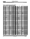
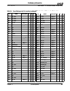
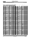
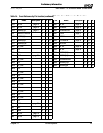

76 Pin Descriptions Chapter 11
AMD Athlon™ XP Processor Model 10 Data Sheet 26237C—May 2003
Preliminary Information
INTR Pin
INTR is an input from the system that causes the processor to
start an interrupt acknowledge transaction that fetches the 8-bit
interrupt vector and starts execution at that location.
JTAG Pins
TCK, TMS, TDI, TRST#, and TDO are the JTAG interface.
Connect these pins directly to the motherboard debug connector.
Pull TDI, TCK, TMS, and TRST# up to V
CC_CORE
with pullup
resistors.
K7CLKOUT and
K7CLKOUT# Pins
K7CLKOUT and K7CLKOUT# are each run for two to three
inches and then terminated with a resistor pair: 100 ohms to
V
CC_CORE
and 100 ohms to VSS. The effective termination
resistance and voltage are 50 ohms and V
CC_CORE
/2.
Key Pins
These 16 locations are for processor type keying for forwards and
backwards compatibility (G7, G9, G15, G17, G23, G25, N7, Q7, Y7,
AA7, AG7, AG9, AG15, AG17, AG27, and AG29). Motherboard
designers should treat key pins like NC (No Connect) pins. A
socket designer has the option of creating a top mold piece that
allows PGA key pins only where designated. However, sockets
that populate all 16 key pins must be allowed, so the motherboard
must always provide for pins at all key pin locations.
See “NC Pins“ for more information.
NC Pins
The motherboard should provide a plated hole for an NC pin. The
pin hole should not be electrically connected to anything.
NMI Pin
NMI is an input from the system that causes a non-maskable
interrupt.
PGA Orientation Pins
No pin is present at pin locations A1 and AN1. Motherboard
designers should not allow for a PGA socket pin at these
locations.
For more information, see the
AMD Athlon™ Processor-Based
Motherboard Design Guide
, order# 24363.
PLL Bypass and Test
Pins
PLLTEST#, PLLBYPASS#, PLLMON1, PLLMON2,
PLLBYPASSCLK, and PLLBYPASSCLK# are the PLL bypass and
test interface. This interface is tied disabled on the motherboard.
All six pin signals are routed to the debug connector. All four
processor inputs (PLLTEST#, PLLBYPASS#, PLLMON1, and
PLLMON2) are tied to V
CC_CORE
with pullup resistors.
PWROK Pin
The PWROK input to the processor must not be asserted until
all voltage planes in the system are within specification and all
system clocks are running within specification.
For more information, Chapter 9, “Signal and Power-Up
Requirements” on page 43.