


Chapter 3 Signals and Pinout Tables
38 Reference Manual COM 830
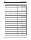
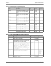
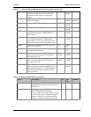
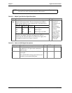
C-D Connector Signal Descriptions
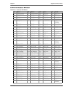
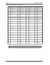
A4
3
USB2+ B43 USB3+ A98 VCC_12V B98 TV_DAC_
B
A4
4
USB_2_3_OC# B44 USB_0_1_OC# A99 VCC_12V B99 TV_DAC_
C
A4
5
USB0- B45 USB1- A10
0
GND (FIXED) B10
0
GND
(FIXED)
A4
6
USB0+ B46 USB1+ A10
1
VCC_12V B10
1
VCC_12V
A4
7
VCC_RTC B47 EXCD1_PERST# A10
2
VCC_12V B10
2
VCC_12V
A4
8
EXCD0_PERST# B48 EXCD1_CPPE# A10
3
VCC_12V B10
3
VCC_12V
A4
9
EXCD0_CPPE# B49 SYS_RESET# A10
4
VCC_12V B10
4
VCC_12V
A5
0
LPC_SERIRQ B50 CB_RESET# A10
5
VCC_12V B10
5
VCC_12V
A5
1
GND (FIXED) B51 GND (FIXED) A10
6
VCC_12V B10
6
VCC_12V
A5
2
PCIE_TX5+ B52 PCIE_RX5+ A10
7
VCC_12V B10
7
VCC_12V
A5
3
PCIE_TX5- B53 PCIE_RX5- A10
8
VCC_12V B10
8
VCC_12V
A5
4
GPI0 B54 GPO1 A10
9
VCC_12V B10
9
VCC_12V
A5
5
PCIE_TX4+ B55 PCIE_RX4+ A11
0
GND (FIXED) B11
0
GND
(FIXED)
NOTE The signals marked with an asterisk symbol (*) are not supported on the COM 830.
PCIE_TX5± and PCIE_RX5± are used for the onboard Gigabit Ethernet and
therefore are not available.
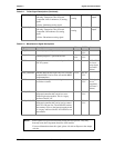
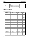
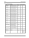
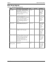
Table 3-17. PCI Signal Descriptions
Signal Description I/O PU/PD Comment
PCI_AD[0:31] PCI bus multiplexed address and data lines I/O
3.3V
PCI_C/BE[0:3]# PCI bus byte enable lines, active low I/O
3.3V
PCI_DEVSEL# PCI bus Device Select, active low I/O
3.3V
PU 8k2
3.3V
PCI_FRAME# PCI bus Frame control line, active low I/O
3.3V
PU 8k2
3.3V
PCI_IRDY# PCI bus Initiator Ready control line, active
low
I/O
3.3V
PU 8k2
3.3V
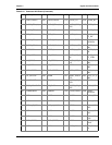
Table 3-16. Connector A-B Pinout (Continued)