


AD620
REV. E
–10–
V
B
–V
S
A1 A2
A3
C2
R
G
R1
R2
GAIN
SENSE
GAIN
SENSE
R3
400⍀
10k⍀
10k⍀
I2
I1
10k⍀
REF
10k⍀
+IN
– IN
20A
20A
R4
400⍀
OUTPUT
C1
Q2
Q1
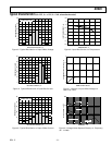
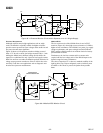
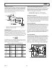
Figure 33. Simplified Schematic of AD620
THEORY OF OPERATION
The AD620 is a monolithic instrumentation amplifier based on
a modification of the classic three op amp approach. Absolute
value trimming allows the user to program gain accurately (to
0.15% at G = 100) with only one resistor. Monolithic construc-
tion and laser wafer trimming allow the tight matching and
tracking of circuit components, thus ensuring the high level of
performance inherent in this circuit.
The input transistors Q1 and Q2 provide a single differential-
pair bipolar input for high precision (Figure 33), yet offer 10×
lower Input Bias Current thanks to Superβeta processing. Feed-
back through the Q1-A1-R1 loop and the Q2-A2-R2 loop main-
tains constant collector current of the input devices Q1, Q2
thereby impressing the input voltage across the external gain
setting resistor R
G
. This creates a differential gain from the
inputs to the A1/A2 outputs given by G = (R1 + R2)/R
G
+ 1.
The unity-gain subtracter A3 removes any common-mode sig-
nal, yielding a single-ended output referred to the REF pin
potential.
The value of R
G
also determines the transconductance of the
preamp stage. As R
G
is reduced for larger gains, the transcon-
ductance increases asymptotically to that of the input transistors.
This has three important advantages: (a) Open-loop gain is
boosted for increasing programmed gain, thus reducing gain-
related errors. (b) The gain-bandwidth product (determined by
C1, C2 and the preamp transconductance) increases with pro-
grammed gain, thus optimizing frequency response. (c) The
input voltage noise is reduced to a value of 9 nV/√Hz, deter-
mined mainly by the collector current and base resistance of the
input devices.
The internal gain resistors, R1 and R2, are trimmed to an abso-
lute value of 24.7 kΩ, allowing the gain to be programmed
accurately with a single external resistor.
The gain equation is then
G =
49.4 kΩ
R
G
+ 1
so that
R
G
=
49.4 kΩ
G − 1
........................................
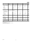
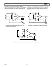
........................................
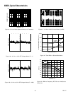
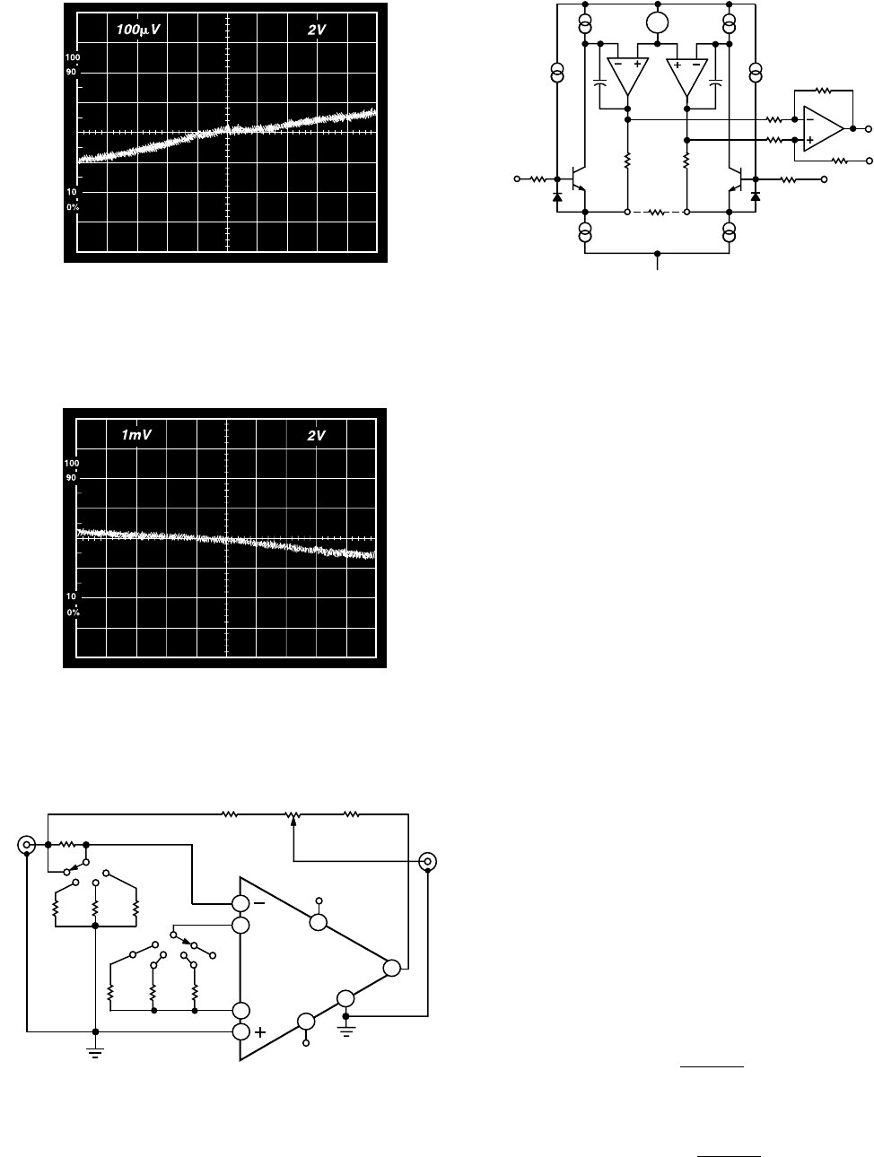
Figure 31b. Gain Nonlinearity, G = 100, R
L
= 10 k
Ω
(100
µ
V = 10 ppm)
........................................
........................................
Figure 31c. Gain Nonlinearity, G = 1000, R
L
= 10 k
Ω
(1 mV = 100 ppm)
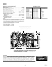
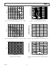
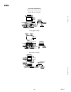
AD620
V
OUT
G=1
G=1000
49.9⍀
10k⍀*
1k⍀
10T
10k⍀
499⍀
G=10
G=100
5.49k⍀
+V
S
11k⍀ 1k⍀ 100⍀
100k⍀
INPUT
10V p-p
–V
S
*ALL RESISTORS 1% TOLERANCE
7
1
2
3
8
6
4
5
Figure 32. Settling Time Test Circuit