


AD620
REV. E
–13–
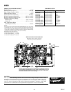
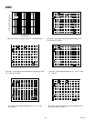
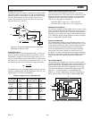
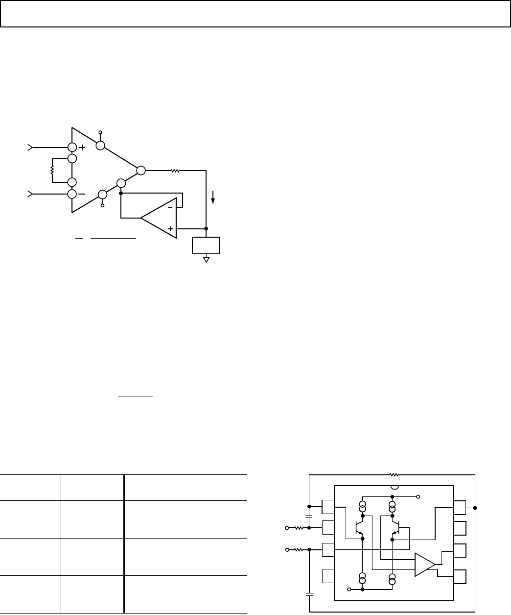
Precision V-I Converter
The AD620, along with another op amp and two resistors, makes
a precision current source (Figure 37). The op amp buffers the
reference terminal to maintain good CMR. The output voltage
V
X
of the AD620 appears across R1, which converts it to a
current. This current less only, the input bias current of the op
amp, then flows out to the load.
AD620
R
G
–V
S
V
IN+
V
IN–
LOAD
R1
I
L
V
x
I =
L
R1
=
IN+
[(V ) – (V )] G
IN–
R1
6
5
+ V –
X
4
2
1
8
3
7
+V
S
AD705
Figure 37. Precision Voltage-to-Current Converter
(Operates on 1.8 mA,
±
3 V)
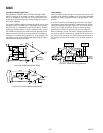
GAIN SELECTION
The AD620’s gain is resistor programmed by R
G
, or more pre-
cisely, by whatever impedance appears between Pins 1 and 8.
The AD620 is designed to offer accurate gains using 0.1%–1%
resistors. Table II shows required values of R
G
for various gains.
Note that for G = 1, the R
G
pins are unconnected (R
G
= ∞). For
any arbitrary gain R
G
can be calculated by using the formula:
R
G
=
49.4 kΩ
G − 1
To minimize gain error, avoid high parasitic resistance in series
with R
G
; to minimize gain drift, R
G
should have a low TC—less
than 10 ppm/°C—for the best performance.
Table II. Required Values of Gain Resistors
1% Std Table Calculated 0.1% Std Table Calculated
Value of R
G
, ⍀ Gain Value of R
G
, ⍀ Gain
49.9 k 1.990 49.3 k 2.002
12.4 k 4.984 12.4 k 4.984
5.49 k 9.998 5.49 k 9.998
2.61 k 19.93 2.61 k 19.93
1.00 k 50.40 1.01 k 49.91
499 100.0 499 100.0
249 199.4 249 199.4
100 495.0 98.8 501.0
49.9 991.0 49.3 1,003
INPUT AND OUTPUT OFFSET VOLTAGE
The low errors of the AD620 are attributed to two sources,
input and output errors. The output error is divided by G when
referred to the input. In practice, the input errors dominate at
high gains and the output errors dominate at low gains. The
total V
OS
for a given gain is calculated as:
Total Error RTI = input error + (output error/G)
Total Error RTO = (input error × G) + output error
REFERENCE TERMINAL
The reference terminal potential defines the zero output voltage,
and is especially useful when the load does not share a precise
ground with the rest of the system. It provides a direct means of
injecting a precise offset to the output, with an allowable range
of 2 V within the supply voltages. Parasitic resistance should be
kept to a minimum for optimum CMR.
INPUT PROTECTION
The AD620 features 400 Ω of series thin film resistance at its
inputs, and will safely withstand input overloads of up to ±15 V
or ±60 mA for several hours. This is true for all gains, and power
on and off, which is particularly important since the signal
source and amplifier may be powered separately. For longer
time periods, the current should not exceed 6 mA (I
IN
≤
V
IN
/400 Ω). For input overloads beyond the supplies, clamping
the inputs to the supplies (using a low leakage diode such as an
FD333) will reduce the required resistance, yielding lower
noise.
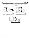
RF INTERFERENCE
All instrumentation amplifiers can rectify out of band signals,
and when amplifying small signals, these rectified voltages act as
small dc offset errors. The AD620 allows direct access to the
input transistor bases and emitters enabling the user to apply
some first order filtering to unwanted RF signals (Figure 38),
where RC Ϸ 1/(2 πf) and where f ≥ the bandwidth of the
AD620; C ≤ 150 pF. Matching the extraneous capacitance at
Pins 1 and 8 and Pins 2 and 3 helps to maintain high CMR.
–IN
1
2
3
4
5
6
7
8
R
R
+IN
C
C
R
G
Figure 38. Circuit to Attenuate RF Interference