


ADSP-2181/ADSP-2183
REV. 0
–13–
ESD SENSITIVITY
The ADSP-2181 is an ESD (electrostatic discharge) sensitive device. Electrostatic charges readily
accumulate on the human body and equipment and can discharge without detection. Permanent
damage may occur to devices subjected to high energy electrostatic discharges.
The ADSP-2181 features proprietary ESD protection circuitry to dissipate high energy discharges
(Human Body Model). Per method 3015 of MIL-STD-883, the ADSP-2181 has been classified as
a Class 2 device.
Proper ESD precautions are recommended to avoid performance degradation or loss of function-
ality. Unused devices must be stored in conductive foam or shunts, and the foam should be
discharged to the destination before devices are removed.
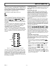
WARNING!
ESD SENSITIVE DEVICE
ADSP-2181 TIMING PARAMETERS
GENERAL NOTES
Use the exact timing information given. Do not attempt to de-
rive parameters from the addition or subtraction of others.
While addition or subtraction would yield meaningful results for
an individual device, the values given in this data sheet reflect
statistical variations and worst cases. Consequently, you cannot
meaningfully add up parameters to derive longer times.
TIMING NOTES
Switching characteristics specify how the processor changes its
signals. You have no control over this timing—circuitry external
to the processor must be designed for compatibility with these
signal characteristics. Switching characteristics tell you what the
processor will do in a given circumstance. You can also use switch-
ing characteristics to ensure that any timing requirement of a
device connected to the processor (such as memory) is satisfied.
Timing requirements apply to signals that are controlled by cir-
cuitry external to the processor, such as the data input for a read
operation. Timing requirements guarantee that the processor
operates correctly with other devices.
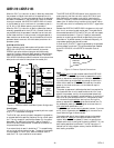
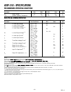
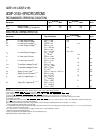
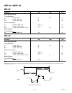
MEMORY TIMING SPECIFICATIONS
The table below shows common memory device specifications
and the corresponding ADSP-2181 timing parameters, for your
convenience.
Memory ADSP-2181 Timing
Device Timing Parameter
Specification Parameter Definition
Address Setup to t
ASW
A0–A13, xMS Setup before
Write Start
WR Low
Address Setup to t
AW
A0–A13, xMS Setup before
Write End
WR Deasserted
Address Hold Time t
WRA
A0–A13, xMS Hold after
WR Deasserted
Data Setup Time t
DW
Data Setup before WR
High
Data Hold Time t
DH
Data Hold after WR High
OE to Data Valid t
RDD
RD Low to Data Valid
Address Access Time t
AA
A0–A13, xMS to Data Valid
xMS = PMS, DMS, BMS, CMS, IOMS
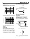
FREQUENCY DEPENDENCY FOR TIMING
SPECIFICATIONS
t
CK
is defined as 0.5t
CKI
. The ADSP-2181 uses an input clock
with a frequency equal to half the instruction rate: a 16.67 MHz
input clock (which is equivalent to 60 ns) yields a 30 ns proces-
sor cycle (equivalent to 33 MHz). t
CK
values within the range of
0.5t
CKI
period should be substituted for all relevant timing pa-
rameters to obtain the specification value.
Example: t
CKH
= 0.5t
CK
– 7 ns = 0.5 (30 ns) – 7 ns = 8 ns
ABSOLUTE MAXIMUM RATINGS
*
Supply Voltage . . . . . . . . . . . . . . . . . . . . . . . . . . –0.3 V to +7 V
Input Voltage . . . . . . . . . . . . . . . . . . . . . –0.3 V to V
DD
+ 0.3 V
Output Voltage Swing . . . . . . . . . . . . . . –0.3 V to V
DD
+ 0.3 V
Operating Temperature Range (Ambient) . . . .–40°C to +85°C
Storage Temperature Range . . . . . . . . . . . . . –65°C to +150°C
Lead Temperature (5 sec) TQFP . . . . . . . . . . . . . . . . +280°C
Lead Temperature (5 sec) PQFP . . . . . . . . . . . . . . . . . +280°C
*
Stresses above those listed under “Absolute Maximum Ratings” may cause
permanent damage to the device. These are stress ratings only, and functional
operation of the device at these or any other conditions above those indicated in the
operational sections of this specification is not implied. Exposure to absolute
maximum rating conditions for extended periods may affect device reliability.
ADSP-2181