


ADSP-2181/ADSP-2183
REV. 0
–4–
• SPORTs support serial data word lengths from 3 to 16 bits
and provide optional A-law and µ-law companding according
to CCITT recommendation G.711.
• SPORT receive and transmit sections can generate unique in-
terrupts on completing a data word transfer.
• SPORTs can receive and transmit an entire circular buffer of
data with only one overhead cycle per data word. An interrupt
is generated after a data buffer transfer.
• SPORT0 has a multichannel interface to selectively receive
and transmit a 24 or 32 word, time-division multiplexed, se-
rial bitstream.
• SPORT1 can be configured to have two external interrupts
(
IRQ0 and IRQ1) and the Flag In and Flag Out signals. The
internally generated serial clock may still be used in this
configuration.
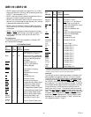
Pin Descriptions
The ADSP-2181/ADSP-2183 is available in 128-lead TQFP
and 128-lead PQFP packages.
PIN DESCRIPTIONS
#
Pin of Input/
Name(s) Pins Output Function
Address 14 O Address Output Pins for Program,
Data, Byte, & I/O Spaces
Data 24 I/O Data I/O Pins for Program and
Data Memory Spaces (8 MSBs
Are Also Used as Byte Space
Addresses)
RESET 1 I Processor Reset Input
IRQ2 1 I Edge- or Level-Sensitive
Interrupt Request
IRQL0,
IRQL1 2 I Level-Sensitive Interrupt
Requests
IRQE 1 I Edge-Sensitive Interrupt
Request
BR 1 I Bus Request Input
BG 1 O Bus Grant Output
BGH 1 O Bus Grant Hung Output
PMS 1 O Program Memory Select Output
DMS 1 O Data Memory Select Output
BMS 1 O Byte Memory Select Output
IOMS 1 O I/O Space Memory Select Output
CMS 1 O Combined Memory Select Output
RD 1 O Memory Read Enable Output
WR 1 O Memory Write Enable Output
MMAP 1 I Memory Map Select Input
BMODE 1 I Boot Option Control Input
CLKIN,
XTAL 2 I Clock or Quartz Crystal Input
#
Pin of Input/
Name(s) Pins Output Function
CLKOUT 1 O Processor Clock Output.
SPORT0 5 I/O Serial Port I/O Pins
SPORT1 5 I/O Serial Port 1 or Two External
IRQs, Flag In and Flag Out
IRD, IWR 2 I IDMA Port Read/Write Inputs
IS 1 I IDMA Port Select
IAL 1 I IDMA Port Address Latch
Enable
IAD 16 I/O IDMA Port Address/Data Bus
IACK 1 O IDMA Port Access Ready
Acknowledge
PWD 1 I Powerdown Control
PWDACK 1 O Powerdown Control
FL0, FL1,
FL2 3 O Output Flags
PF7:0 8 I/O Programmable I/O Pins
EE 1 * (Emulator Only*)
EBR 1 * (Emulator Only*)
EBG 1 * (Emulator Only*)
ERESET 1 * (Emulator Only*)
EMS 1 * (Emulator Only*)
EINT 1 * (Emulator Only*)
ECLK 1 * (Emulator Only*)
ELIN 1 * (Emulator Only*)
ELOUT 1 * (Emulator Only*)
GND 11 – Ground Pins
VDD 6 – Power Supply Pins
*These ADSP-2181/ADSP-2183 pins must be connected only to the EZ-ICE
connector in the target system. These pins have no function except during
emulation, and do not require pull-up or pull-down resistors.
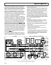
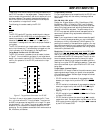
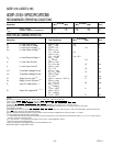
Interrupts
The interrupt controller allows the processor to respond to the
eleven possible interrupts and reset with minimum overhead.
The ADSP-2181/ADSP-2183 provides four dedicated external
interrupt input pins,
IRQ2, IRQL0, IRQL1, and IRQE. In addi-
tion, SPORT1 may be reconfigured for
IRQ0, IRQ1, FLAG_IN
and FLAG_OUT, for a total of six external interrupts. The ADSP-
2181/ADSP-2183 also supports internal interrupts from the timer,
the byte DMA port, the two serial ports, software, and the
power-down control circuit. The interrupt levels are internally
prioritized and individually maskable (except power down and
reset). The
IRQ2, IRQ0, and IRQ1 input pins can be programmed
to be either level- or edge-sensitive.
IRQL0 and IRQL1 are level-
sensitive and
IRQE is edge sensitive. The priorities and vector
addresses of all interrupts are shown in Table I, and the inter-
rupt registers are shown in Figure 7.