


Evaluation Board User Guide UG-001
Rev. 0 | Page 3 of 24
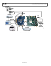
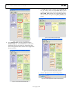
EVALUATION BOARD HARDWARE
The AD9272/AD9273 evaluation board provides all of the support
circuitry required to operate the AD9272/AD9273 in its various
modes and configurations. Figure 2 shows the typical bench
characterization setup used to evaluate the ac performance of
the AD9272/AD9273. It is critical that the signal sources used for
the analog input and clock have very low phase noise (<1 ps rms
jitter) to realize the optimum performance of the signal chain.
Proper filtering of the analog input signal to remove harmonics
and lower the integrated or broadband noise at the input is
necessary to achieve the specified noise performance (see the
AD9272 or AD9273 data sheet).
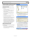
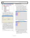
See the Evaluation Board Software Quick Start Procedures section
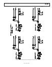
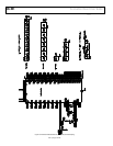
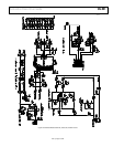
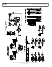
to get started and Figure 21 to Figure 31 for the complete sche-
matics and layout diagrams that demonstrate the routing and
grounding techniques that should be applied at the system level.
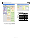
POWER SUPPLIES
This evaluation board comes with a wall-mountable switching
power supply that provides a 6 V, 2 A maximum output. Connect
the supply to the rated 100 V ac to 240 V ac wall outlet at 47 Hz
to 63 Hz. The other end is a 2.1 mm inner diameter jack that
connects to the PCB at P701. Once on the PC board, the 6 V
supply is fused and conditioned before connecting to low dropout
linear regulators that supply the proper bias to each of the various
sections on the board.
When operating the evaluation board in a nondefault condition,
L705, L706, L707, and L709 can be removed to disconnect the
switching power supply. This enables the user to bias each section
of the board individually. Use P602 and P603 to connect a different
supply for each section. At least one 1.8 V supply is needed with
a 1 A current capability for AVDD_DUT and DRVDD_DUT;
however, it is recommended that separate supplies be used for
both analog and digital domains. An additional supply is also
required to supply 3.0 V to the device under test, AVDD2_DUT.
This should also have a 1A current capability. To operate the
evaluation board using the SPI and alternate clock options, a
separate 3.3 V analog supply is needed in addition to the other
supplies. The 3.3 V supply, or AVDD_3P3V, should have a 1 A
current capability.
To bias the crosspoint switch circuitry or CW section and
differential gain drive circuitry, separate +5 V and −5 V supplies
are required at P601. These should each have 1 A current capability.
This section cannot be biased from a 6 V, 2 A wall supply. Separate
supplies are required at P601.
INPUT SIGNALS
When connecting the clock and analog source, use clean signal
generators with low phase noise, such as Rohde & Schwarz SMA or
HP8644B signal generators or the equivalent. Use a 1 m, shielded,
RG-58, 50 Ω coaxial cable for making connections to the evalu-
ation board. Enter the desired frequency and amplitude (refer to
the specifications in the AD9272 or AD9273 data sheet). The
evaluation board is set up to be clocked from the crystal oscil-
lator, OSC401.
If a different or external clock source is desired, follow the
instructions Clock Circuitry section. Typically, most Analog
Devices evaluation boards can accept ~2.8 V p-p or 13 dBm sine
wave input for the clock. When connecting the analog input
source, it is recommended to use a multipole, narrow-band
band-pass filter with 50 Ω terminations. Analog Devices uses
TTE and K&L Microwave, Inc., band-pass filters. The filter
should be connected directly to the evaluation board.
OUTPUT SIGNALS
The default setup uses the FIFO5 high speed, dual-channel
FIFO data capture board (HSC-ADC-EVALCZ). Two of the
eight channels can then be evaluated at the same time. For more
information on channel settings on these boards and their optional
settings, visit www.analog.com/FIFO.