


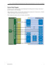
Connect Tech Xtreme/SBC PCIe/104 Single Board Computer and PCIe/104 Qseven Carrier Board - User Manual
Revision 0.02
11
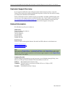
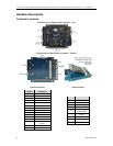
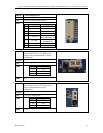
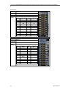
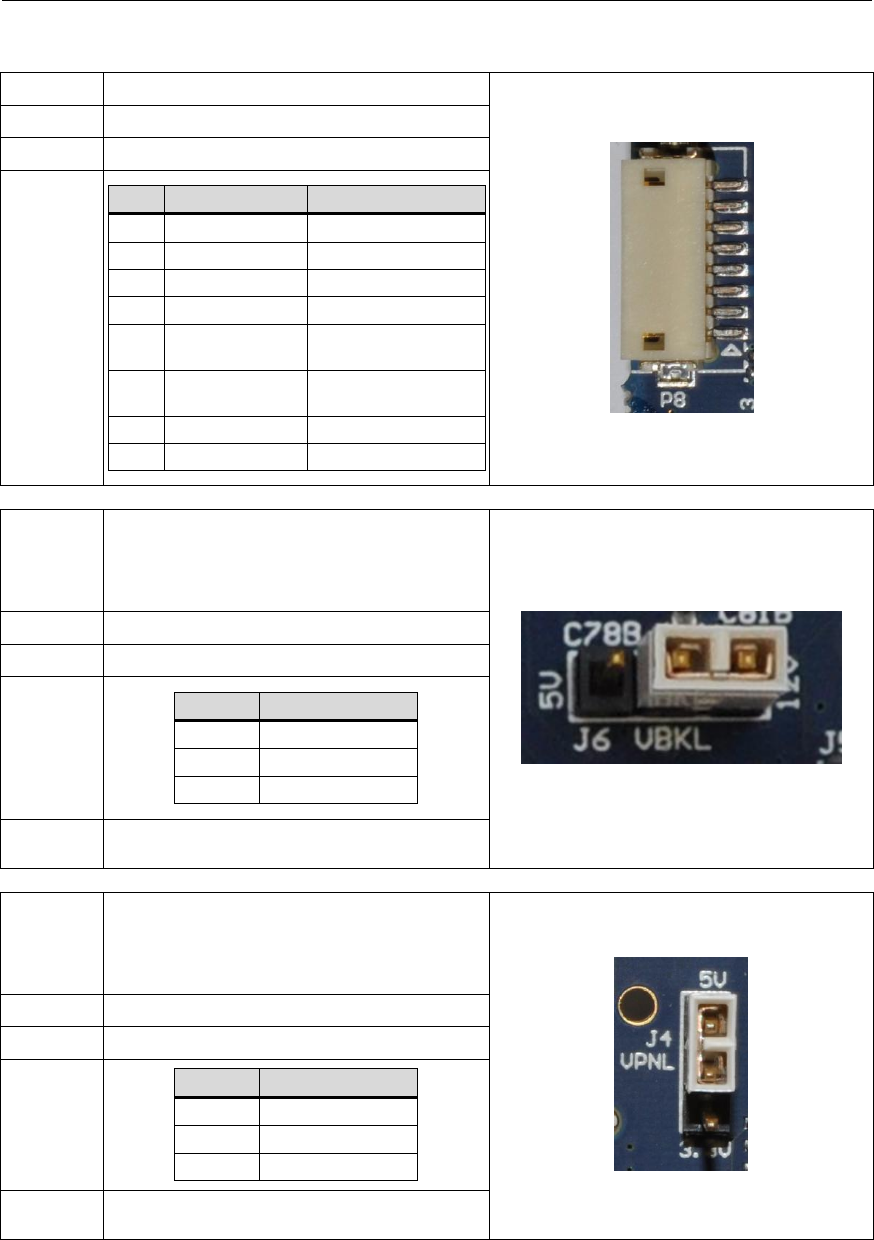
Function
LVDS backlight power
Location
P8
Type
Hirose DF13-8P-1.25H connector
Pinout
Pin
Signal
Description
1
+12V
+12 V DC, max. 1A
2
+12V
+12 V DC, max. 1A
3
+5V
+5 V DC, max. 1A
4
+5V
+5 V DC, max. 1A
5
LVDS_BLEN
Backlight enable,
level selected with J4
6
VCC_BKL
Back light power,
selected with J6
7
GND
Digital ground
8
GND
Digital ground
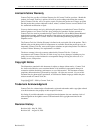
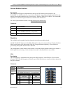
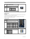
Function
LVDS backlight power select
Selects either +12V or +5V. Refer to the
display panel’s documentation for proper
configuration.
Location
J6
Type
1x3 0.100” jumper block
Pinout
Position
Description
1-2
+12V
2-3
+5V
off
floating
Default
+12V
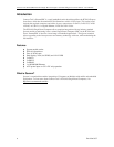
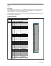
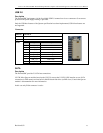
Function
LVDS panel power select
Selects either +3.3V or +5V. Refer to the
display documentation for proper
configuration.
Location
J4
Type
1x3 0.100” jumper block
Pinout
Position
Description
1-2
+5V
2-3
+3.3V
off
floating
Default
+3.3V
* Note the silk screen labels +5V and +3.3V are reversed on Revision A.