


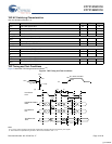

CY7C1318CV18
CY7C1320CV18
Document Number: 001-07160 Rev. *F Page 6 of 26
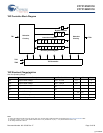
Functional Overview
The CY7C1318CV18, and CY7C1320CV18 are synchronous
pipelined Burst SRAMs equipped with a DDR interface, which
operates with a read latency of one and half cycles when DOFF
pin is tied HIGH. When DOFF pin is set LOW or connected to
V
SS
the device behaves in DDR I mode with a read latency of
one clock cycle.
Accesses are initiated on the rising edge of the positive input
clock (K). All synchronous input timing is referenced from the
rising edge of the input clocks (K and K
) and all output timing is
referenced to the rising edge of the output clocks (C/C
, or K/K
when in single clock mode).
All synchronous data inputs (D
[x:0]
) pass through input registers
controlled by the rising edge of the input clocks (K and K
). All
synchronous data outputs (Q
[x:0]
) pass through output registers
controlled by the rising edge of the output clocks (C/C
, or K/K
when in single-clock mode).
All synchronous control (R/W, LD, BWS
[0:X]
) inputs pass through
input registers controlled by the rising edge of the input clock (K).
CY7C1318CV18 is described in the following sections. The
same basic descriptions apply to CY7C1320CV18.
Read Operations
The CY7C1318CV18 is organized internally as two arrays of
512K x 18. Accesses are completed in a burst of two sequential
18-bit data words. Read operations are initiated by asserting
R/W
HIGH and LD LOW at the rising edge of the positive input
clock (K). The address presented to address inputs is stored in
the read address register and the least significant bit of the
address is presented to the burst counter. The burst counter
increments the address in a linear fashion. Following the next K
clock rise, the corresponding 18-bit word of data from this
address location is driven onto Q
[17:0]
, using C as the output
timing reference. On the subsequent rising edge of C the next
18-bit data word from the address location generated by the
burst counter is driven onto Q
[17:0]
. The requested data is valid
0.45 ns from the rising edge of the output clock (C or C
, or K and
K
when in single clock mode, 200 MHz and 250 MHz device). To
maintain the internal logic, each read access must be allowed to
complete. Read accesses can be initiated on every rising edge
of the positive input clock (K).
The CY7C1318CV18 first completes the pending read transac-
tions, when read access is deselected. Synchronous internal
circuitry automatically tristates the output following the next rising
edge of the positive output clock (C). This enables a seamless
transition between devices without the insertion of wait states in
a depth expanded memory.
Write Operations
Write operations are initiated by asserting R/W
LOW and LD
LOW at the rising edge of the positive input clock (K). The
address presented to address inputs is stored in the write
address register and the least significant bit of the address is
presented to the burst counter. The burst counter increments the
address in a linear fashion. On the following K clock rise the data
presented to D
[17:0]
is latched and stored into the 18-bit write
data register, provided BWS
[1:0]
are both asserted active. On the
subsequent rising edge of the negative input clock (K
) the infor-
mation presented to D
[17:0]
is also stored into the write data
register, provided BWS
[1:0]
are both asserted active. The 36 bits
of data are then written into the memory array at the specified
location. Write accesses can be initiated on every rising edge of
the positive input clock (K). This pipelines the data flow such that
18 bits of data can be transferred into the device on every rising
edge of the input clocks (K and K
).
When Write access is deselected, the device ignores all inputs
after the pending write operations are completed.
Byte Write Operations
Byte write operations are supported by the CY7C1318CV18. A
write operation is initiated as described in the Write Operations
section. The bytes that are written are determined by BWS
0
and
BWS
1
, which are sampled with each set of 18-bit data words.
Asserting the appropriate Byte Write Select input during the data
portion of a write latches the data being presented and writes it
into the device. Deasserting the Byte Write Select input during
the data portion of a write enables the data stored in the device
for that byte to remain unaltered. This feature can be used to
simplify read/modify/write operations to a byte write operation.
Single Clock Mode
The CY7C1318CV18 can be used with a single clock that
controls both the input and output registers. In this mode the
device recognizes only a single pair of input clocks (K and K) that
control both the input and output registers. This operation is
identical to the operation if the device had zero skew between
the K/K
and C/C clocks. All timing parameters remain the same
in this mode. To use this mode of operation, tie C and C
HIGH at
power on. This function is a strap option and not alterable during
device operation.
DDR Operation
The CY7C1318CV18 enables high-performance operation
through high clock frequencies (achieved through pipelining) and
double data rate mode of operation. The CY7C1318CV18
requires a single No Operation (NOP) cycle when transitioning
from a read to a write cycle. At higher frequencies, some appli-
cations may require a second NOP cycle to avoid contention.
If a read occurs after a write cycle, address and data for the write
are stored in registers. The write information must be stored
because the SRAM cannot perform the last word write to the
array without conflicting with the read. The data stays in this
register until the next write cycle occurs. On the first write cycle
after the read(s), the stored data from the earlier write is written
into the SRAM array. This is called a posted write.
If a read is performed on the same address on which a write is
performed in the previous cycle, the SRAM reads out the most
current data. The SRAM does this by bypassing the memory
array and reading the data from the registers.
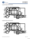
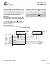
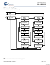
Depth Expansion
Depth expansion requires replicating the LD control signal for
each bank. All other control signals can be common between
banks as appropriate.
[+] Feedback